This kind of system control method is not suitable for applications such as precise motion control (such as precise control of the rotational speed of the motor with varying load) because they require a short communication delay between the controller and the equipment, but it requires a highly synchronous system level control. Accurate control of the entire system (such as a speed change), such as a large printing plant or a long automated production line, is useful. If there is enough time for each device to issue an instruction, the only constraint on such clock-based control accuracy is system-wide clock synchronization accuracy. Several industrial networking standards (not just Internet-based standards) are using the IEEE 1588 standard to provide this control capability. IEEE 1588 provides a highly accurate master clock and a validated clock synchronization mechanism that can be used to generate all local clocks and maintain very accurate system-level synchronization with the master clock. Ethernet-based networks are favored for their low cost and ease of implementation of Ethernet. Ethernet switches are key components that help these advantages, and enterprise systems rely heavily on them for high-performance and easy-to-maintain infrastructures. This huge enterprise market for switches means that they are easy to implement and inexpensive, but most switches on the market today are not designed for low latency performance or deterministic routing times, and are therefore difficult to use in industrial environments. The IEEE 1588 system synchronizes the master and slave clocks by detecting the communication delay between the master and the slave. Placing a switch between the master and slave clocks introduces additional delay because the switch must analyze the packets and then route them. The increased delay is not a good thing, but it can be corrected for delays, so it is not a major issue. The biggest problem is that as traffic increases, the time required to route packets will increase dramatically. This is due to the time required to cache, analyze, and route packets to many destinations. This change greatly reduces the accuracy of the 1588 clock synchronization, which significantly deteriorates the real-time control performance of the entire system. The measurement of the delay between 1588 master and slave clocks also depends on the symmetry of the communication time in both directions because the measurement method used is to count a time stamped message from the slave clock to the master clock and then back from the master clock to the slave clock. The time used is divided by 2. In most switch and Ethernet network implementations, this symmetry is less likely to occur, further reducing clock synchronization accuracy. However, the IEEE 1588 standard provides a solution to this problem: If the switch itself also has a clock (shown in Figure 1), it can measure the time required for packet routing and integrate it into the synchronization calculation. Because the system does not need this functionality, switches that contain such 'boundary' clocks are difficult to see, and are generally expensive, and are often customized for specific network implementations. With the rapid proliferation of IEEE 1588-based networks, manufacturers face daunting challenges in how to implement IEEE 1588 functionality efficiently and cost-effectively in product and network infrastructures. Developing a custom ASIC solution is possible, but with the rise of ASIC development costs and rapid changes in industrial Ethernet standards, the development of such programs is slow, risky, and not cost-effective. Solutions can also be developed for each protocol using microprocessors and third-party ASICs or ASSPs for specific network protocols, but this means implementing a separate solution for each network standard, which is also costly and inefficient. These solutions may also face the problem of lack of flexibility and equipment quickly out of date. At present, designers can only avoid the above restrictions by carefully implementing networks, minimizing the use of switches, or minimizing real-time network traffic. This network isolation measure can achieve acceptable performance levels for some applications, but they are difficult to implement or maintain. Save development time Implementing IEEE 1588-enabled switches with FPGAs is the ideal solution to this problem. Directors of Altera, National Semiconductor and MorethanIP have combined their expertise to provide an optimized eight-port switch design for industrial Ethernet designers. This design can reduce engineering development time by six to nine months. The savings in development time will enable device manufacturers to take the lead in time to market. Figure 2 shows a development board with embedded IEEE 1588 capabilities developed by Altera's Stratix II FPGA based on the MorethanIP enterprise system. The reference design attached to this development board implements IEEE 1588-compliant switches in a simple and cost-effective way, and is easily modified to cater to other systems and rapidly changing market demands. These advantages are achieved through the flexibility of the FPGA and a 32-bit RISC processor integrated in the FPGA design. The Ethernet MAC core and switching core intellectual property (IP) with 1588 timing control and programmable uplink functions was developed by MorethanIP GmbH. The MorethanIP Enterprise System also provides UDP and 1588 software stacks that can run on a 32-bit Altera Nios II RISC processor soft core. To provide the best physical interface, the eight-port switch design uses four dual-port PHY transceivers from National Semiconductor Enterprise Systems. The reference design has less than 100ns clock synchronization capability and can be used in a variety of applications. This level of accuracy is critical to meeting the demanding communication delays and quality of service (QoS) requirements for industrial connectivity. Target applications include switches using different industry standards such as Ethernet/IP, ProfiNet, Ethernet Powerlink, and other Ethernet protocols. Extend product life cycle The FPGA's programmability is the key to the above design advantages. From a single hardware platform, designers can easily implement switches that support different industrial Ethernet protocols (such as EtherCAT, ProfiNet, etc.). The board can support different industrial Ethernet protocols within the same system or from the same Ethernet port. This is achieved by implementing different media access controller (MAC) hardware modules and embedded processor software to support different Ethernet standards and IEEE 1588 functions. The ability to easily reuse previously designed capabilities and the availability of off-the-shelf IP means that FPGA-based designs can generate a configuration that supports new features in a very short time compared to designs using ASIC or ASSP devices. The FPGA loads hardware configuration and embedded processor software from a serial flash. Even after the device is delivered to the site during production, it is easy to change the hardware and software functions of the FPGA by rewriting the contents of the flash memory. The programmable hardware and software processing power within the FPGA means that designers can integrate the additional functionality they need through applications that are hardware or software. The ability to implement new functions by simply reprogramming the FPGA is a guarantee of the future of the product (such as support for IEEE 1588 v2.0), and new features can be presented to customers very quickly. Because of the long lifecycle of FPGAs, device manufacturers do not have to worry about the risk of potential device termination. Since the design is based on IP, porting the design to next-generation FPGAs is also more convenient, making it possible for designers to benefit from the lower cost or greater performance of next-generation FPGA products. Coupled with the ease of on-site upgrades, FPGA implementation becomes the best way to easily support product development throughout the product cycle. This reference design uses Altera's Stratix II FPGAs, which allow all Nios II processor code to be stored in on-chip memory, although lower-cost systems can be implemented using the Altera Enterprise System's Cyclone III family of FPGA devices. Embedded Switch Matrix IP Figure 3 shows the embedded eight-port switch fabric of MorethanIP GmbH's enterprise system. It contains 8 10/100 Mbps MACs that conform to the Ethernet 802.3 specification and each MAC supports IEEE 1588, which means that it can use programmable timing. The local synchronous high-accuracy clock is time-stamped for each incoming 1588 data frame. To implement the boundary clock application, the switch design implements both IEEE 1588 V1 master and slave applications. The port that communicates with the host is automatically configured as a slave port. The embedded 1588 application generates a precise clock from the slave port and forwards the clock information to other ports that are automatically configured as master. Tight integration with programmable timers ensures that the clock is synchronized to the master clock within 100 ns. Within the switch, up to two priority queues can be implemented per port to provide Quality of Service (QoS) guarantees for critical services. The switch can also programmatically identify and prioritize traffic using a 3-bit VLAN priority field, a 6-bit DiffServ Layer 3 code point (IPv4), or an 8-bit service class (IPv6). The switch is designed to support IEEE 1588 Release 1 boundary and Release 2 transparent clock applications. The design can be further modified and enhanced to add custom logic, such as the addition of bridged application software on legacy system or PCI and other different system interfaces to facilitate the integration of switches into existing systems. In this design, the Nios II embedded processor supports the IP configuration and management of the switch, and can run the User Datagram Protocol (UDP) stack, the IEEE 1588 protocol stack, and precise timing synchronization, and supports dual 10/100 PHY transceiving. The PHY management and line diagnostics of the device (as shown in Figure 4). Embedded processors can also be used for high-level networking functions such as running spanning tree and rapid spanning tree algorithms and terminating TCP/IP links. Spanning Tree Protocol (STP) and Rapid Spanning Tree Protocol (RSTP) are link management protocols that support path redundancy to prevent unwanted loops in the network (so that industrial Ethernet networks work properly, only between two nodes. There can be a valid path). PHY transceiver Each transceiver has two completely independent 10/100Mbps ports for multi-port applications, as shown in Figure 5. The transceiver's port switching also allows the two ports to be configured to provide fully integrated range expansion, media conversion, fast hardware-based failover, and port monitoring. The device incorporates multi-port support for a common industrial Ethernet topology. In particular, designers need redundant support for different applications and need to be able to handle failover under a variety of conditions. Switching from one network stack to another requires no less than a few hundred milliseconds, but some applications, such as security applications, require a failover that is extremely fast, preferably at the PHY layer. The transceiver in this reference design switches from one port to another in ns, even though the host still manages the control path. The architectural improvements in the transceiver signal path far exceed the minimum PHY layer specification requirements, and can completely solve design issues such as jitter and latency. Each Ethernet PHY layer is driven by a reference clock. In order to minimize jitter, the PHY layer specification requires an extremely accurate clock with accuracy within 50 PPM of the transceiver's 25 MHz reference clock. In addition, in order to meet the specification requirements, the starting jitter must be very small. To solve this problem, a mechanism that tolerates more jitter is integrated within the architecture. The device architecture also optimizes latency performance for real-time Ethernet operations to ensure that switch latency is minimized. In many real-time system implementations, Ethernet packet data transmission delay is an important parameter for normal system operation, and fixed or variable delay in the Ethernet PHY will become an important component of system delay calculation. section. The PHY transceiver is designed to limit the variation of the received data delay, which provides a very deterministic system delay. Because the receive data is aligned with the receive clock, the non-deterministic factors that are typically encountered when the device receives data are circumvented. Therefore, the device can provide very deterministic receive data delay in MII and RMII modes. In addition, the transceiver can reduce the non-deterministic possibilities common in sending RMII delays. Another important design feature is the built-in cable diagnostics feature that adds a forward-looking diagnostic capability to the transceiver's traditional time domain reflectometry (TDR) approach. The newly created fault isolation feature can use the transceiver's powerful signal processing capabilities to track link quality while data is being transferred. This robust TDR implementation is to send pulses out of the receive or transmit wire pairs and observe the results on both wire pairs. By observing the type and intensity of the reflected signal on each pair of lines, and calculating by software, the short-circuit and open-circuit conditions of the cable and the distance of the fault point can be determined, and it can be determined which pair has the problem and the pair offset. Proactively monitoring and correcting changes or deteriorating link quality can reduce system downtime and save expensive maintenance costs. This function can also detect failures during installation and save a lot of debugging man-hours. This article summary Industrial Ethernet technology has been advancing and becoming more and more popular, and designers are facing increasingly strong demand for cost-effective industrial switches. Since ASIC and ASSP-based switches are fixed in their architecture, there is virtually no room for customization of new system features. In order to increase the design of features, it is generally necessary to overhaul them. This will lead to additional design time and cost. However, FPGA designs that support IEEE 1588 switches as described above can save engineering time by 6 to 9 months, and provide designers with the flexibility they need to help them implement the Precision Timing Protocol (PTP) and support multiple industrial Ethernet standards. , additional standard interfaces or other possible custom features.
As a single sided PCB manufacturer, Jinghongyi PCB has been single sided PCB for many years. Production and manufacturing experience, with a very exquisite single sided PCB Manufacturing process flow chart.
Basically, there is no challenge for PCB manufacturer to produce single sided PCB and the technology is quite mature nowadays. The main focus for PCB manufacturer is how to control production cost and save more cost for customers.
It is the type of a single layer PCB which is made up a rigid material such as fiber glass. These PCBs are inflexible and prevent the circuit from bending and breaking. Currently these are used in different types of devices such as in calculators and power supplies etc.
It is the type of a single layer PCB which is mode out a flexible material instead of a rigid material and for this purpose plastic materials are used. It has so many advantages over single layer rigid pub but it fabrication cost is so much high.
It is the type of a single layer PCBs which is used for high frequency circuits normally in giga hertz. These PCBs are made out a Teflon or polyphenylene oxide (PPO) material. During choosing high frequency single layer PCB many aspects are keep in mind such as dielectric loss, thermal expansion and water absorption etc.
It the type of single layer PCBs which is made out by the combination of plastic and fiber glass. Both materials are combined together into single layer. It has so many advantages over single layer rigid and flexible PCB such as it reduces the weight and size of overall PCB.
single sided vs double sided PCB
Single Sided PCB Single Sided PCB, Single Layer PCB, 1 Layer PCB, making circuit boards JingHongYi PCB (HK) Co., Limited , https://www.pcbjhy.com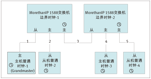
Figure 1: Typical Boundary Clock Application Diagram 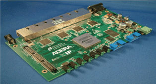
Figure 2: Eight-port switch development board with IEEE 1588 timing control 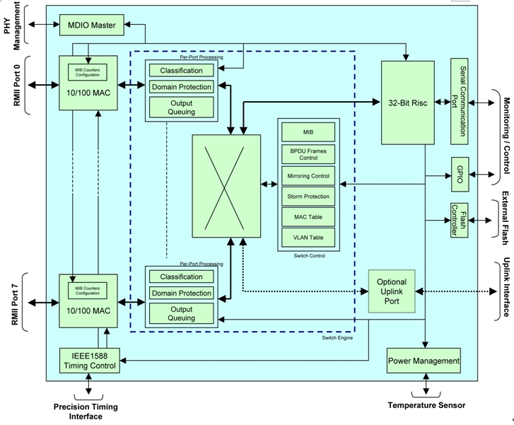
Figure 3: Block Diagram of MorethanIP's Eight-Port Switch Compliant with the IEEE 1588 Standard 
Figure 4: IEEE 1588 block diagram including software and hardware 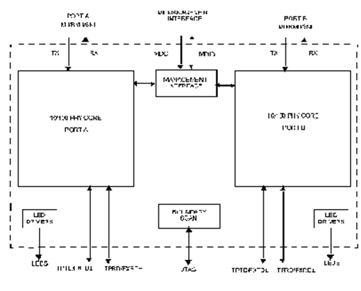
Figure 5: National Semiconductor's PHY Transceiver Block Diagram
The Single Most Important Thing You Need To Know About Single Sided PCB
We can produce single sided copper PCB, single sided copper clad PCB Board , single sided Flex PCB .
We know that when you choose single sided PCB manufacturer, product quality is one of the first factors you need to consider. We are not only engaged in PCB manufacturing for many years, but also one of the large-scale PCB manufacturers in China. We can not only produce single sided PCB, but also Double Sided PCB , Multilayer PCB , Aluminum PCB and so on.
In addition to product quality, you may also need to consider the single sided PCB price factor. If you choose us as your partner, you can rest assured that we will be able to provide you with not the best price on the premise of guaranteeing product quality, but the price that we both feel is very reasonable. What do you think?
In this article, we will elaborate on the definition, type, cost components, structure, advantages and disadvantages, manufacturing process and raw materials of single sided PCB. Finally, we will introduce the application of single sided PCB and the differences between single sided PCB and double sided PCB. And how to choose between single sided PCB and double sided PCB.
What Is Single Sided PCB

Single-sided PCB diagram mainly used Network Printing(Screen Printing), that is, resist on copper surface, After etching, mark the welding resistance, and then finish the hole and the shape of the part by punching.
Fundamentally, single-sided and double-sided Printed Circuit Boards serve the same purpose. Both serve as catalysts for electrical connections between components, however there are some key differences that set them apart from each other. More specifically, they differ in the costs associated with production and development processes, as well as ampacity differences.
With the appearance of electronic transistor, single sided PCB was developed in the early of 1950, which is mainly manufactured in USA. Single-sided PCB was manufactured by copper etching directly at that time. During 1953 to 1955, Japan use imported copper make out paper phenolic aldehyde copper substrate, and apply mainly on radio products. In 1956, single-sided PCB technology was made big progress with the appearance of professional PCB manufacturers from Japan. In the early stage, copper substrate mainly used paper phenolic aldehyde, but because paper phenolic aldehyde with the factors of low electric insulation, bad solder thermal stability, twist issue etc, paper epoxide resin and glass fiber epoxy resin was developed soon after. Currently, paper epoxide resin is widely used in consuming electronic.
Types of Single Layer PCB
It the type of single layer PCB which is made out with aluminum material substrate. The design of this PCB is almost same as copper backed PCB but only difference is that, in these PCBs aluminum substrate is used instead of copper. Aluminum backed is used with thermal insulating material for transferring the heat from insulating material to back.
What Goes Into Determining single sided PCB Costs and price
No matter whether manufacturing a single-sided PCB, double-sided PCB, or multilayer PCB, three main cost categories exist: Primary production costs, dependent costs, and overhead costs.
Often, single layer PCB are used for simple devices and usually cheaper than multilayer PCB.
Multilayer PCB has one or multiple conductor patterns inside the board, this increases the area available for wiring. multilayer PCB, such as 4 Layer PCB , 6 Layer PCB and 8 Layer PCB are usually used for more complicated devices. For example, smart phones use 12 layers due to the various demands of the circuit. As a result, multilayer PCB circuit boards are more expensive.
You can break them down into the following categories:

Layout alters the cost balance. While the number and size of holes remain the same with single-sided PCBs, two different circuit designs on one substrate change the number of holes and add vias.
Because double-sided PCBs welcome complex circuit designs, layout also becomes a dependent factor. As the number of traces increase, costs increase. Smaller surface mount components fastened to the bottom side change the trace spacing. As the space between the traces narrows, costs can jump 5 to 10 percent.
Different layouts may require different hole sizes and the use of laser rather than mechanical drills. Smaller hole sizes and larger hole counts drive the cost higher because of a change in the manufacturing process.
Advantages of Single Sided PCB

Single Layer PCB Disadvantages
Despite their cost advantages and other perks, single-layer boards are not the right choice for every project due to the limitations they have, which include:
How to make single sided PCB

Single sided PCB manufacturing Process flow chart
One thin layer of thermally conductive but electrically insulating dielectric is laminated with copper. Soldermask is usually applied on top of the copper.
Cutting - Cleaning - Drilling - Cleaning - PTH - Panel - Plating - Cleaning - Photolithography - Image Transfer - Inspection - Copper/Tin - Plating - Coating - Removing/Etching/Tin - Removing - Inspection - Cleaning - Solder - Mask - Exposure/Develop/Inspection - Prepreg - Screen - HASL - Conformal - Coating - Post - Soldering - Cleaning - Test - Final Inspection - Packing
Single layer PCB Raw Material
Construction of Single Sided PCB


The base material, which is also named as substrate, is composed of insulating fiber glass which gives PCB strength and compact look. The nature and type of base material defines if board is going to be Flexible PCB or Rigid PCB.
Above substrate, there lies a copper layer which provides conducting path for various components on the board. The copper thickness is different for different boards depending on your needs and requirements and is defined in ounces per square foot.
On the top of copper foil, there exists a solder mask layer. This layer is mainly used for protection and makes the copper foil insulating which helps in avoiding the conduction in case direct contact happens with some conducting material.
On the top of all layers, there exists a silkscreen layer that is mainly used for adding symbols and characters on the board so a common person can anticipate the clear understanding of the board.
Single Sided PCB Applications

What Is Double Sided PCB

It need circuits on both sides. Via is the holes on boards, coated with metal and it can connect wires on both sides. Because the area of Double-sided PCB is twice as large as the Single-sided PCB, and because the wiring is interleaved, which is better suited for circuits that are more complex.
Someone may feel confused that if one Double-sided PCB, wires on both sides while Electronic parts only one side, is this a Double-sided board or a single onel? The answer is obvious. This kind of board is a Double-sided board, it's just install a component on the Double-sided board.
Differences Between Single sided PCB and Double sided PCB

Single and double sided printed circuit boards share the same material make-up: FR-4, which is a form of fiberglass mixed with epoxy. In modern manufacturing, this is usually layered with copper for conductivity and then coated in solder mask for a professional finish. Sometimes, in a process called silk screening, industrial printers print markings and labels on the board as well.
Single-sided PCBs consist of the FR4 insulating core substrate and a thin layer of copper coating on the bottom or solder-side of the substrate. Through-hole components mount on the top or component-side of the substrate with the leads passing through to the bottom side and soldered to the copper pads and tracks. Surface mount components mount directly to the solder side. The primary difference between the two boards will be in conductor placement.
Double-sided boards rely on the same core substrate but have conductors on both sides of the substrate. Very simply, a double-sided board delivers twice the area for conductors. Complex routing can occur with through-hole components mounted on the top layer and surface mount components mounted on the bottom layer. Plated through holes establish [vias" or the electrical connections between the two sides.
Choose Single Sided PCB or Double Sided PCB?
Which PCB you pick depends on your needs and requirements. Sometimes single sided PCBs are more suitable for project design as compared to double sided PCBs and vice versa.
Before you pick any type of PCB for your project, you must take one thing into consideration that single sided PCB layouts are more difficult to route as compared to double sided PCB, but following are the reasons why you should put an effort for making and picking single sided PCB over other PCBs.
Relationship Resources
Multilayer Metal Core PCB
Single Layer Metal Core PCB
Single Sided Flexible PCB
Using FPGA to Design Optimization of Industrial Ethernet Switches
An increasingly popular countermeasure against the non-deterministic communication time of the Ethernet protocol is to implement a local clock within each device. Since most devices have a microprocessor and a (relatively) high-speed clock, this method is easier to implement. If the precise clock synchronization can be achieved and maintained throughout the entire network while controlling the precise operation timing of the entire system, then the only limitation of this method is the communication delay and system-wide clock synchronization accuracy.