In today's increasingly competitive business environment, whether products are easy to upgrade on the spot and whether they are easy to use flexibly become a key factor for businesses to quickly capture the market. Against this backdrop, FPGA devices based on SRAM LUT structures developed by Alter have been widely used. Field Programmable Gate Array (FPGA) is a high-density programmable logic device. The logic function is realized by configuring the generated data file into the static configuration data memory (SRAM) inside the chip. Repeatable programmability allows flexible implementation of various logic functions. Due to the volatile nature of the SRAM, data must be reconfigured every time the system is powered on, ie, ICR (In-Circuit Reconfigurability). Only when the data is correctly configured, the system can work normally. Therefore, an external ROM is required to save its configuration data. The configuration of the FPGA is time-sequential. If the FPGA itself cannot control the configuration timing, external configuration devices are needed to perform timing control. Taking Altera's FPGA as an example, because it cannot control the timing itself, there is a dedicated EPC series configuration device for its use. In an embedded system, since it contains a microprocessor, a microprocessor can be used to generate the configuration timing and the configuration data stored in the system ROM can be stored in the FPGA. Therefore, it is not necessary to use a dedicated EPC series configuration device to configure the FPGA. This not only saves costs, but also effectively reduces the system volume. This article focuses on the configuration of FPGAs in embedded systems. 2. How FPGA Devices Are Configured The ICR-enabled FPGA devices produced by Altera Corporation are FLEX6000, FLEX10K, APEX, and ACEX series, which can be configured in the following ways: 1. Use dedicated EPC configuration devices such as EPC16, EPC8, EPC2, EPC1; The following detailed analysis of the above five configuration methods. When EPC is used to configure the device, the configuration file is first downloaded from the computer to the EPC configuration device, and then the EPC configuration device controls the configuration timing to configure the FPGA. The EPC configuration device has one programmable and two erasable programming types: one programmable chip can only be written once, which is not suitable for repeated debugging, modification, and convenient upgrade of the product in the development phase; the erasable programming type is expensive and With limited capacity, for large-capacity programmable logic devices, multiple chip configurations are required to configure the daisy-chain, which increases the difficulty of system design. When using PS, PPS, PPA configuration, the configuration file is stored in the system ROM in binary form beforehand, and then the configuration data is sent to the FPGA through the microprocessor. The PS is sent to the FPGA in a serial manner and the PPS is sent to the FPGA in parallel. The FPGA internally converts parallel data into serial data, which requires externally configured clock drivers. Compared with PS and PPS, the configuration time used is almost the same, but the interface mode of PS is relatively simple, so the embedded system usually chooses PS mode to configure the FPGA. When using PPA to configure data, the microprocessor sends the configuration data to FPAG in parallel and then serializes the data within the FPGA. The difference from PPS is that there is no need to configure an external clock driver for serialization, but the interface is more complex and rarely used in engineering. The boundary scan method needs to be connected to a computer and cannot be used in the field. This method is rarely used in embedded systems. Through the above analysis, when using an FPGA in an embedded system, a dedicated EPC configuration device, PS, PPS, PPA can be used, but PS, PPS, and PPA have more cost and volume advantages than dedicated EPC configurations. In PS, PPS, PPA, PS is the optimal communication method. Therefore, in the embedded system, PS passive serial mode is usually selected to configure the FPGA. 3. FPGA configuration circuit design in embedded system 3.1. PS Mode Configuration Timing In the embedded system, the microprocessor can generate the configuration timing, can communicate with the FPGA directly, and transfer the configuration file in the ROM to the SRAM of the FPGA. The FPGA is usually configured using the PS passive serial mode. The following describes the configuration timing of the five signal lines used in the communication. The five signal lines are nCONFIG, nSTATUS, CONF_DONE, DCLK, and DATA, respectively, and are connected to the microprocessor's five I/O ports and corresponding FPGA pins. The five I/O ports on the microprocessor connect the above five signal lines. Which connect nCONFIG, DCLK, DATA port is set to output state, nSTATUS, CONF_DONE port is set to input state. When the microprocessor starts to communicate with the FPGA, the microprocessor first sends a negative pulse greater than 8 μm on nCONFIG and detects the signal on nSTATUS. When the FPGA receives a falling edge on nCONFIG, it quickly pulls nSTATUS and CONF_DONE low and holds the signal low until nCONFIG rises high. When nCONFIG rises high after 1μm, nSTATUS also raises the level. After the microprocessor detects a change in nSTATUS, it assumes that the FPGA is ready to receive data. Next, the microprocessor will generate a configuration clock pulse. The first rising edge of the configured clock is at least 1 μm later than the rising edge of nSTATUS. Since the configuration data is synchronized with the rising edge of the configuration clock, the data line must already have a configuration data signal before the rising edge of the configuration clock occurs. The configuration data is sent to the data line in the order of the low order and the high order. After all data has been transferred, the CONF_DONE line is raised to indicate that the configuration is complete. If an exception occurs during transmission, the FPGA forces nSTATUS to pull low and the microprocessor will restart the configuration once it detects this phenomenon. Since the configuration file already contains some code that is initialized by the FPGA, after the configuration file is transferred, the FPGA can work normally. 3.2 Configuration Circuit Design The PS circuit configuration mode of the FPGA in the embedded system is shown in Figure 2. The left microprocessor and FLASH, SDRAM form a basic embedded system. FLASH is the program's memory, which stores the system's entire application, configuration program, and configuration files. SDRAM as a system program running space can effectively solve the microprocessor's own small SRAM capacity. 4. System software design Programs stored in the FLASH include system programs, configuration programs, and configuration files. After the system is powered on, the microprocessor starts running from the boot program at address 0 of the FLASH. After the system is initialized, the microprocessor moves the application program in the FLASH to the SDRAM for operation. Since most of embedded systems currently use real-time multitasking operating systems, the configuration program should be placed in the first running task to ensure that it starts to run after startup. The software design is based on the timing requirements of the microprocessor and FPGA communication signal lines. First initialize the port of the microprocessor and generate a 20μm negative pulse on the P0 pin. Read the signal on the P4 pin. If it is high, start data preparation, read the data, and serialize the data by shifting. The bit stream sends the lower data to the P1 pin and generates a rising clock edge through P2. Because the rising edge of the clock is synchronized with the data transfer, the signal on the P1 pin is passed to the FPGA. Then read the data right shift, put the lower bit on the P1 pin, and then generate a clock rising edge on P2. If this cycle continues, the next byte is read when the read-out of one byte is completed, and it is transmitted in the same manner. At the same time when data transmission is detected, whether P4 (nSTATUS) is low or not, if an error is encountered during the transmission, P4 will be low, so that the system needs to be reconfigured. Wait until the data is transmitted and check the status of P3 pin. If it is high, it indicates that the configuration is successful. If it is low, it means that the configuration fails and the system needs to be reconfigured. Software design language can choose C, also can use assembly. In the development process, according to the characteristics of the hardware of the chip, attention is paid to optimization in various aspects. Because the speed of reading data from SDRAM in the embedded system is very fast, the software design does not need to consider the transmission speed problem from SDRAM to the microprocessor. When writing data to an FPGA device, the least significant bit first. The configuration timing generated by the microprocessor can be achieved by sending high and low levels to the timing pins. 5 Conclusion Today's embedded systems have been applied to various fields, so no matter the cost or volume optimization, it is very necessary. Using the resource advantages of the embedded system to complete the special functions of other components can effectively achieve the effect of optimizing integration and reducing costs. The general solution discussed in this article is applicable to different microprocessors and all related serial FPGA products of Altera Corporation. Since the FPGA has a reconfigurable function, a plurality of configuration files with different functions may be pre-configured in the embedded system, and the corresponding configuration may be performed according to the needs of the site. This fully demonstrates the design concept of FPGA field upgrades and flexible use.
Advantages:
1 .Light weight Wire Cable Tray,Wire Cable Tray Systems,Wire Tray,Mesh Type Cable Tray Jiangsu Loncin Electric Equipment Co.,Ltd , https://www.loncincabletray.com
2. Passive Serial Mode (PS) using the microprocessor's serial interface;
3. Passive parallel synchronization method (PPS), using the microprocessor's parallel synchronization interface;
4. Passive parallel asynchronous mode (PPA), using the microprocessor's parallel asynchronous interface;
5. Boundary-scan mode (JTAG) using JTAG download cable. 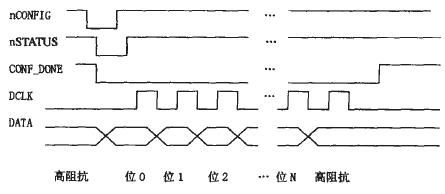
Figure 1 PS mode configuration signal timing diagram 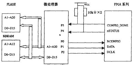
2.Durability
3.High Strength
4. anti-corrosive, non-conducting, electro-magnetic transparency
5.Easy to cut and Install
6.fire retardant.
7.Low thermal expansion coefficient, good thermal insulation.
8. Easily forming and maintenance convenient.
9.Can be designed based on customer's drawings
Discussion on Configuration of FPGA Device in Embedded System
1 Introduction