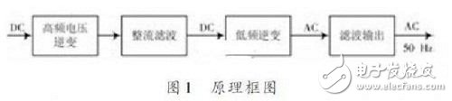
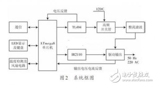
0 Preface In the wind power industry, it is often necessary to repair the wind turbines in the field. At this time, it is necessary to supply power for various maintenance tools and instruments. Therefore, design a portable. Low power consumption. Intelligent sinusoidal inverter power supply is necessary to supply these devices, which can greatly improve the efficiency of maintenance fans. This paper is based on this situation and is designed based on a single-chip intelligent sinusoidal inverter power supply. 1 sinusoidal inverter power supply design The inverter designed in this paper is a portable power converter capable of converting DC 12V DC into 220V sinusoidal AC voltage and providing it to general electrical appliances. At present, low-voltage small-power inverter power supplies have been widely used in industrial and civil fields. Especially in transportation. Field measurement and control operations. Where electromechanical engineering repairs cannot directly use the mains, low-voltage low-power inverter power supply becomes one of the necessary tools. It only needs to have a battery with sufficient power to connect with it, which can generate the AC voltage required by general electrical appliances. . Due to the working environment of the low-voltage and low-power inverter power supply, it is in the wilderness or the environment is bad. There is a lot of interference, so the design requirements for it are relatively high, so it must have a small size. Light weight. low cost. High reliability. Strong anti-interference. Good electrical performance and other characteristics. In response to these characteristics and requirements, a simple and practical sine wave inverter power supply is studied, which meets the actual requirements with low-cost, affordable and simple components, which will be widely welcomed by the market. At present, there are various schemes for designing low-power inverter power supplies. The early design scheme is to directly control the DC voltage with a double-switch tube, and generate a 220V square wave inverter voltage under the action of a 50Hz square wave. However, with the continuous improvement of the requirements of the power supply equipment for the performance of the inverter power supply, the square wave inverter power supply has been eliminated in most occasions, and the application of the sine wave inverter has become an inevitable trend. Now, there are three main designs for low-power sine wave inverters on the market. 1.1 Inverted sine wave inverter power supply In this scheme, the DC voltage to be inverted is directly applied to the double-switch tube, and then the sinusoidal pulse width modulation pulse train of several tens of times 50 Hz is directly used to drive the switch tube, and then the output voltage is subjected to "smoothing" processing. In order to obtain a continuously varying waveform similar to a sine wave, the advantage of this method is that the circuit is inverted once, which is efficient and simple. But the transformer is too bulky and there is no way to meet the requirements of small size and light weight. 1.2 Multiple inverter sine wave inverter power supply The scheme divides the 50Hz signal of the driving switch into several driving signals with different phases and the same frequency, respectively driving the respective switching tubes, so that the respective output voltages are also shifted by a certain phase, and then superimposed and outputted with multiple steps. The staircase wave is filtered again to output the desired sine wave voltage. The circuit of this kind of scheme is more complicated. Once a group of switch tubes fails, the output waveform has great distortion. 1.3 Secondary inverter sine wave inverter power supply With the maturity of high-frequency switching tube technology, the circuit design of the inverter power supply tends to be firstly transformed, and then the frequency conversion is first converted into a high-frequency alternating current, and then the high-frequency alternating current is converted into a 50 Hz sinusoidal alternating current power supply. The principle block diagram is shown in Figure 1. Since the price of the switch tube is low, the unit circuit constituting FIG. 1 is cost-effective, and most of the low-power inverter power sources are currently produced on the market with such a design scheme. 2 Sinusoidal inverter power supply based on single chip control Among the three inverter power supply design schemes listed above, a secondary inverter sine wave inverter power supply is preferred. According to this idea, the early specific circuit solutions mostly use PWM control chips such as TL494, SG3524, SG3525A, etc., to control the DC/DC and DC/AC part of the switch tube at a fixed frequency, and use the correction circuit to output the waveform. Make corrections to meet the sine wave requirements. But this pure PWM chip controls the circuit for aging of components. fever. If the interference is not automatically corrected, or the correction capability is poor, it often causes circuit failures in actual applications. With the development of single-chip technology, designers constantly want to introduce the single-chip microcomputer into the control of the sinusoidal inverter power supply, but for the control of the high-frequency part, the low-cost single-chip computer can not complete this function, and the high-cost single-chip microcomputer will reduce the cost performance, so This paper proposes another design scheme, which is to use a low-cost ATmega8 single-chip microcomputer, with TL494, IR2110 and switch tube to form a sine wave inverter power supply with small size, low cost and strong control capability. The block diagram is shown in Figure 2. It can be seen from Figure 2 that the whole system is mainly controlled by the ATmega8 single-chip microcomputer, and whether the TL494 and IR2110 work, all are adjusted by the single-chip microcomputer according to the feedback signal. The high frequency switch tube and the drive output portion are formed by a single phase full bridge inverter circuit. The specific working principle is to use ATmega8 single-chip microcomputer as the core of system control. The function of high-frequency PWM signal can be generated by TL494. The pulse width of the single-chip microcomputer is controlled and output to control the full-phase inverter circuit composed of high-frequency switch tube. The low DC voltage inverter becomes a high voltage square wave, and after being rectified and filtered, it is sent to the drive output full-bridge inverter circuit. The single-chip microcomputer controls the IR2110 to output the power frequency drive signal, and controls the output drive circuit to output a 50 Hz, 220 V sinusoidal AC voltage. . 3 The specific design of the main circuit The core of the entire inverter system is mainly composed of a single-chip control circuit and a detection circuit. DC/DC conversion circuit. DC / AC output circuit composition. 3.1 DC / DC conversion circuit As shown in Figure 3, the TL494 constitutes a high-frequency pulse output circuit, which uses a pulse width modulation controller TL494 integrated block with excellent performance. The manifold contains a +5V reference supply. Error amplifier, frequency variable sawtooth oscillator. PWM comparator. trigger. Output control circuit. Output transistor and dead time control circuit. The 5th to 6th pins of the integrated block are respectively connected with C1 and R6 to form an RC oscillator circuit, which can drive the TL494 output frequency to 100 pins to control the DCDC terminal in the figure. By controlling the dead time control terminal of the fourth pin, the duty ratio of the output signal can be adjusted to vary from 0 to 49%, thereby controlling the output of the output terminal Q1PWM~Q2PWM, and the P terminal. The VCC terminal and the VFB terminal respectively receive the high-frequency inverter output voltage from the load. The feedback signal of the input voltage is overvoltage with the circuit inside the TL494. The overload protection circuit forms the first level safety protection network of the inverter. Double Burner Electric Hotplate Double Iron Hotplate,Double Burner Electric Hotplate,220V Hotplate,Double Burner Hot Plate Shaoxing Haoda Electrical Appliance Co.,Ltd , https://www.zjhaoda.com