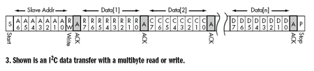
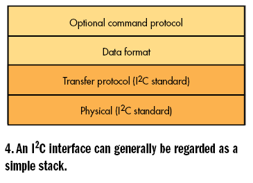
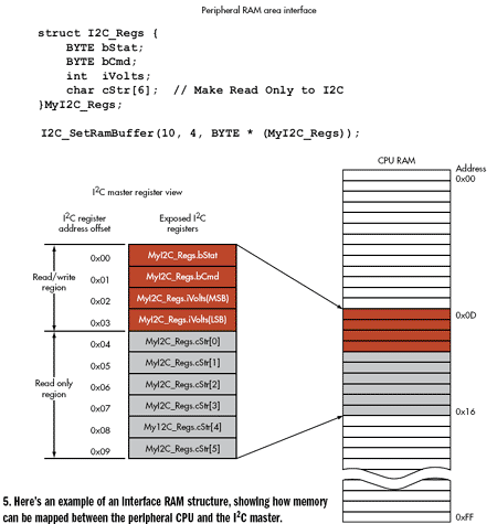
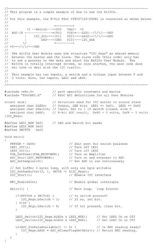
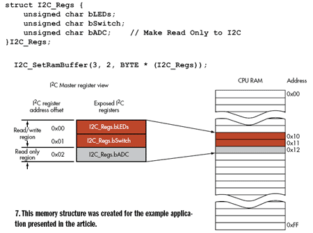
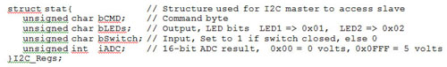
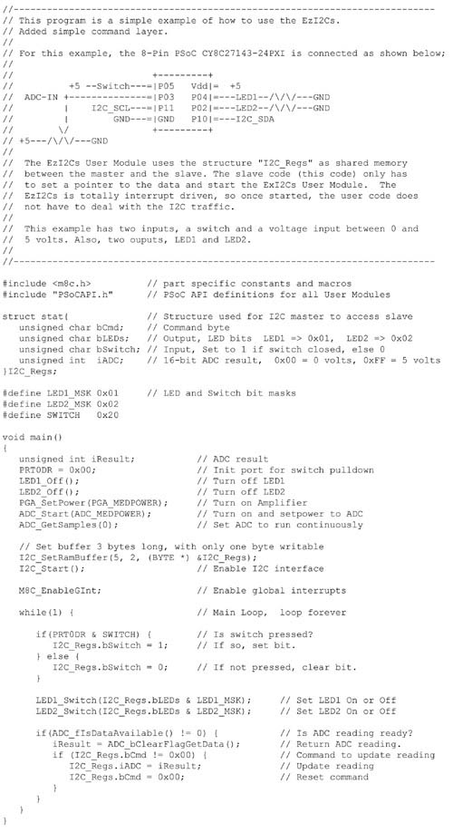
Because of the small number of pins required, a serial interface must be used. Common serial interfaces in processors today include SPI, I2C, USB, and RS-232. By weighing and comparing these interfaces from different aspects, I eventually chose I2C, because it has a simple interface, good flexibility, and is supported by most low-cost controllers. Without the need for very high transmission speeds, fewer pin counts and flow control functions also make the I2C interface more advantageous than the SPI interface. How does I2C work? I2C is a two-wire bidirectional interface that includes a clock signal and a data signal (SCL and SDA). An I2C bus can support up to 12 devices without adding any other signals. The I2C interface specification includes three operating speeds: 100kbps, 400kbps, and 3.4Mbps. Most common controllers only support 100- and 400kbps modes. The I2C bus supports a master device with multiple slave devices or multiple master device configuration structures. One very important feature of I2C is that it supports flow control. If a slave cannot maintain continuous byte transfers, it can suspend the bus until it can keep up with the master's transfer speed. This is useful for slave devices that contain the smallest I2C hardware and must support some of the transport protocols on the firmware. The I2C bus specification supports both addressing protocols 7b and 10b. I have found that the 7b addressing mode is more efficient in most applications. Before we start writing code, we need a good understanding of how the I2C bus works. In any case, the I2C bus must contain at least one master device, at least one or more slave devices. The master always initiates data transfer operations from master to slave. No matter how many peripherals are attached to the bus, the I2C interface has only two signals. Both signals are open-collector and are connected to a Vcc supply via a pull-up resistor of approximately 2.7k. The SDA signal is bidirectional and can be driven by the master or slave device. The SCL signal is driven by the master device, but the slave device must keep the SCL signal low at the end of one data byte to delay the bus until the slave device begins processing the data. The master releases the SCL signal after the last bit of the data byte has been transferred, and then checks if the SCL signal goes high. If SCL does not go high, the master considers the slave to be delaying the master until it begins processing the data. When data is transmitted over the I2C bus, data conversion can only be performed when SCL is low. When the SCL signal is high, the data in any direction should be stable (as shown in Figure 1). When the bus is idle, the master and slave devices do not pull down the SDA and SCL signals. When a data transfer is initiated, the master drives the SDA signal from high to low and the SCL signal is high. In general, the state of the SDA signal remains unchanged when the SCL signal is high, except under start or stop conditions. When the SCL signal is high and the SDA signal goes from low to high, transmission is stopped (as shown in Figure 2). The I2C bus transmits data in units of 8b. Each time a byte is transmitted, it must be confirmed by the data receiver. All data is transmitted starting from the MSB (most significant bit). At the start of each transmission, a START command initiates the transmission, then transmits a 7-bit slave address followed by the R/W flag bit. The I2C standard also supports 10-bit address mode, but the application of this article only requires 7-bit addresses. If a slave recognizes this address, it pulls down the SDA signal during the ACK state and releases it. The R/W flag bit determines the direction of data transfer between the master and slave devices. If the R/W bit is low, data is transmitted from the master device to the slave device. If this bit is high, it means that the slave device reads data from the slave device. All bytes in a packet are transmitted in the same direction. After each byte is transmitted, an ACK is acknowledged by either the master or the slave, depending on the direction of data transfer. Figure 3 shows an example of multibyte read and write. The I2C interface can be seen as a simple stack structure. At the bottom of the stack is the physical layer, which consists of electrical signals. Above the layer is the transmission protocol. It defines the addressing and data transfer methods between the master and slave devices. The third layer from the bottom up is the "data format" layer, which is usually determined by the peripherals. It indicates how the data is stored and addressed in the peripherals. The top level is the "optional command protocol", which is not part of the I2C specification. This layer is user-defined. A possible implementation example will be described later in this article. Since the data format layer depends on the peripherals, each peripheral determines what format data should be stored. Most peripherals have one or more data bytes that can be read or written. Some peripherals even have more than 128 bytes that can be accessed by the master device. In order to optimize the data transfer, we need to design an internal offset mechanism so that when the master device needs to read or write the 100th byte, it does not need to read or write the previous 99 bytes. Therefore, the first byte in the write sequence is always the offset of the data array stored in the peripheral. If more than one byte needs to be written, the second byte is written at the offset determined by the first byte. The offset is relatively constant, which means that if a read is performed after a write sequence, the data being read will start at the offset of the previous write operation. If only one byte is sent in a write sequence, only the offset pointer changes. The real data will not be written to the peripheral (as shown in Figure 4). In Figure 4, the first sequence shows three bytes written to a peripheral from the offset AA. For example, if you have an external byte location that can write data and AA equals 4, then the data will be written to the 5th, 6th and 7th bytes of the sequence, and the offset will be written when the offset is zero. Enter the first byte of the sequence. The second sequence in Figure 4 only writes the offset. The third sequence reads four bytes from the offset "BB". If you execute the third sequence again, it will read the same four bytes. Before the pointer changes, the read operation always starts from the same offset. Peripheral API After defining the interface with the external processor, we need to define the slave device's API. In general, the communication interface must be closely integrated with the application of the peripheral, but what if the application layer does not even need to know the existence of the I2C interface in addition to a few configuration API commands? This way you can easily add I2C interfaces without having to drastically modify the application layer. For example, you can create an interface that accesses external CPU memory through an I2C master device, and the master device only accesses the RAM area allowed by the slave device. The first step is to make the I2C interface run in the background in the form of an Interrupt Service Routine (ISR). This allows the master device to read and write memory operations transparent to the peripheral applications, without polling registers, without redirection or copying data, and without the need to cross-store I2C interface code in the application. The API must be configured to tell the I2C ISR where to put the data, and what data boundaries or lengths it can read and write. However, you do not want the I2C master to access data that it should not access. For example, you don't want the primary device accidentally overwriting the main application stack. The API should tell the interface the location and length of the data. It is best to set the read/write area and read-only area. Figure 5 shows how memory is mapped between the external CPU and the I2C master. The API command "I2C_SetRamBuffer (BufferSize, R/W_Length, DataPointer)" is used to set the BufferSize, R/W_Length, and DataPointer. Data can be stored anywhere in the external CPU RAM space. On the other hand, the I2C master can only see the memory exposed by the API call. Only 10 bytes can be seen in this example, and only the first 4 bytes are writable. Regardless of where the storage buffer is placed, the master sees a sequence of data starting at address 0x00 up to address 0x09. In this example, 10 bytes of data are defined as a structure. Applications use these variables as if they are accessing other addresses or global variables. If you define the structure as global at compile time, most compilers will flatten it so that you don't have to calculate the offset each time you access an element. In other words, using this structure will not generate extra code overhead. achieve After designing the interface between the master and slave devices, the next step is to write some code. Since many high-performance microprocessors support I2C interfaces, many vendors provide I2C-enabled development tools and libraries. We still need to write some of our own code, which will speed up the application development. For example, the Cypress PSoC microcontroller includes some low-level I2C hardware that can be customized through PSoC Designer and a dedicated EzI2C user module. In addition to basic hardware configuration commands, such as I2C_Start() and I2C_Stop() that enable and disable interfaces, a lot of code will be implemented through ISRs (Interrupt Service Routines). The underlying I2C hardware recognizes the Start and Stop conditions of the I2C bus and sets the status flag bits when receiving the slave address and the R/W bit. It does not check for address matching but does this through the firmware. Figure 6 shows the basic firmware flow chart. Note that this flowchart does not contain some hardware details related to specific manufacturer hardware. For many applications where each byte is independent of one another, this interface can meet the requirements. This example includes an 8-pin PSoC CY8C27143-24PXI microcontroller, two LEDs, two LED current limiting resistors, a pushbutton, and a potentiometer for analog variable voltage. Internally, the following components have their own example components: ADC, PGA, two LED drivers, and EzI2C user module. The code listed in this article is the firmware that the user must write for this application. The I2C interface code is handled by the ISR. In this application, the I2C master can monitor the value of the ADC, check the status of the switch, and set the state of the LED. Without having to change the interface again, this interface can be reused on many R&D projects. Figure 7 shows the memory expression down to the true memory location. The project uses 1076B Flash and 19B RAM. The size of the I2C code is approximately 275B, just below the 512B allocated for this interface. Some applications require handshaking between the master and slave devices, not just anonymous data read and write operations. Extending the above interface to perform the handshake operation requires only a small increase in the master and slave device/application code. There are many ways to add this feature. For example, if the result of an ADC conversion exceeds 8b, the host may read the MSB of the ADC conversion and the LSB of the next conversion. If the reading is very stable, then there is no problem. But if the result is between two values, such as 0x0200 and 0x01FF, you may occasionally read 0x02FF. To avoid this problem, we can add a command byte or semaphore. Listing 2 shows the modified structure of the previous example. A new element "bCMD" has been added, and the ADC result variable has changed from 8-bit "bADC" to 16-bit "iADC". In this way, the external firmware does not have to blindly update the ADC's results, but rather waits for the master's commands or semaphores. The command can be any non-zero bCMD value, or the bCMD value can be a wide range of commands that the slave/peripheral can perform. For simplicity, LEDs and switches will continue to be updated. On the other hand, the iADC value is updated only when bCMD is set to a non-zero value. The application now monitors the bCMD. When it is non-zero, it will place the latest ADC result in the iADC and then set bCMD to zero. The master then monitors bCMD and updates the iADC only when bCMD returns to zero. In this way, the master device will never get out of sync ADC results. The rule of the command/semaphore is that the master can set its value and the slave can only clear its value. This is the implementation of the top-level "optional command protocol" mentioned earlier. We don't have to set more complex mechanisms than this. In today's world, the field of solar energy appliacaiton is very important for human being. Belttt's solar power generation system can help people to use the solar energy better. Belttt has divide inverters into AC system and DC system. We are concentrate on off-grid Solar Power System, it makes us more professional. It's build-in inverter and Solar Controller, one piece of device is whole generation system. Solar Power Generator,Solar Generation System,Off Grid Solar Power System,Solar Lighting System Guangzhou City Poojin Electronic Technology Co., Ltd. , https://www.inverter-belttt.com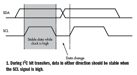


I2C-based processor networking design
Recently, I accepted a task: to develop an interface (software/hardware) that can be easily adapted to multiple applications, and to meet the industry standards commonly used in embedded processors. After analyzing some typical applications, we have listed some design requirements for the hardware interface: commonly used for 32-bit and 8-bit processors; can be supported by commonly used peripheral devices; the amount of peripheral interface code is less than 0.5kB; Smaller number of pins; data bandwidth up to 10kBps; less RAM usage; multiple peripherals supported on one bus; easy to use API; no external interface driver hardware required.