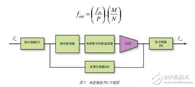
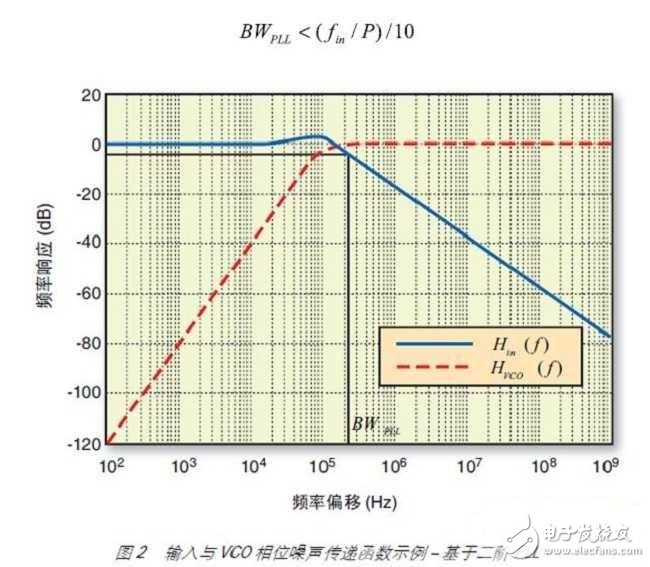
Today's complex FPGAs contain a number of functional blocks for implementing various circuits and systems, such as logic arrays, memory, DSP blocks, processors, phase-locked loops (PLLs) for timing generation, and delay-locked loops (DLLs), standards. I/O, high-speed digital transceivers, and parallel interfaces (PCI, DDR, etc.). These different functional blocks are usually driven by multiple clocks. FPGAs typically use an external oscillator and an internal PLL and DLL to generate the clock. System designers must decide how to combine external and internal resources to achieve the best clock tree design. The programmable clock oscillator is used as a timing reference for FPGA systems and offers a number of advantages. The primary advantage is the design flexibility of high-resolution frequency selection for clock tree optimization. Another great advantage is the spread spectrum modulation that reduces electromagnetic interference (EMI). The intrinsically programmable silicon MEMS clock oscillator architecture can help system designers using FPGAs solve many challenges. This MEMS architecture easily integrates other features such as spread-spectrum clocks for EMI reduction, digitally controlled oscillators for jitter removal, and fail-safe features in high-speed applications. Frequency selection A typical system requires a series of clock frequencies. Some of these are standard frequencies, which may be due to industry-enforced requirements (eg, 100MHz required by PCI Express), or may be due to a wide range of applications (eg, 75MHz for SATA or 33.333 MHz for PCITM). These frequencies are associated with the I/O interface to ensure interoperability because the interfaces may not belong to the same system. In contrast, the user can select the clock frequency used to drive the processor, DSP, and state machine engine to optimize speed, power, or resource usage. When speed optimization is performed, the processing engine should be driven at the highest clock frequency to maximize the number of operations per second. However, the clock period jitter must be low enough to ensure that the minimum clock period is greater than the critical timing path of the design, otherwise logic errors may occur. A common method of frequency selection is to use an internal FPGA PLL to synthesize the high frequency clock from a standard external reference oscillator. This method is only effective if the internal PLL has high frequency resolution and low jitter. Some FPGAs integrate an internal low noise fraction PLL to meet all of these requirements. In this case, a simple external oscillator reference can be used. However, in many cases FPGAs use a PLL with a ring-shaped VCO and an integer feedback divider to combine different frequencies. This PLL is small and flexible, easy to design and control, and has very low power consumption. However, it is difficult to achieve high resolution and low jitter at the same time when using such an internal PLL. Figure 1 shows the general architecture of an integer PLL. Programming the PLL output frequency is done using a prescaler (P), a feedback divider (M), and a postscaler (N), as shown in the following equation: The PLL feedback loop forms a band limited control system. The output period jitter is mainly determined by the reference clock phase noise (PNIn) and the internal VCO phase noise (PNVCO) as shown in the following equation: The input reference clock phase noise and VCO phase noise are closely related to the output phase noise, which are reflected by the low pass filter and the high pass filter response, respectively, such as Hin and HVCO in the expression. HVCO is directly related to the cutoff frequency of Hin. Figure 2 illustrates the relationship between Hin and HVCO in a typical second-order PLL. The highest PLL bandwidth is dependent on the update rate of the phase detector. The maximum actual bandwidth limit for most actual PLLs is as follows: For example, if the PLL input frequency is 40 MHz and P = 40, the highest actual PLL bandwidth is 100 kHz. High Power Light,Led High Power Lamp,High Power Led Light,Led High Power Lamp Price Changxing Fanya Lighting Co.,Ltd , https://www.fyledlights.com