The code segment responsible for reading a single byte of data is shown below: Dj Speaker,Portable Bluetooth Speaker,Lf600 Multifunctional Speaker,Speakers For Large Events NINGBO RFUN AUDIO TECHNOLOGY CO.,LTD , https://www.mosensound.com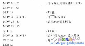
During the read process, T1 is first activated. The RD signal then sends the row address to the address bus (AB), and triggers the flip-flop T1, causing its Q output to go low. This activates RAS (Row Address Strobe) by pulling it low, thereby selecting the appropriate row in the memory array. Next, T0 is set to high, and the RD signal sends the column address to the AB. This generates the CAS (Column Address Strobe) signal, which enables the data from the selected memory cell to be placed on the data bus (DB). The rising edge of the RD signal causes CAS to deactivate. At the same time, the D2 flip-flop is set to 1, which clears D1 and causes RAS to return to a high level. After an RC delay, the data from the addressed cell appears on the DB. Then, D2 is cleared again, and Q2 returns to a high state, resetting D1 and D2 to zero, returning the system to its initial state.
By the end of the read operation, both T0 and T1 are set to low, and RAS and CAS are disabled. This prevents any other read or write operations from interfering with the DRAM, ensuring stable and accurate memory access.
The write process follows a similar sequence, but instead of reading data from the DB, the data is written into the memory cell through the same address lines and control signals. The main difference lies in the direction of data flow and the timing of the signals used to latch the data into the memory array.