The following is the program segment for reading a single byte of data: Midrange Speakers Car Audio,Midbass Speaker,Shopping Mall Conference Speakers,High Performance Broadcast Loudspeaker NINGBO RFUN AUDIO TECHNOLOGY CO.,LTD , https://www.mosensound.com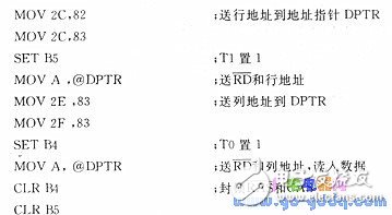
During the read operation, T1 is first set to a high level. The RD signal then sends the row address to the address bus (AB), and triggers the flip-flop latch T1, causing its Q output to go low. This activates the RAS signal (which goes low), thereby performing the row strobe. After that, T0 is set to a high level, and the RD signal sends the column address to AB, generating the CAS signal. This allows the data from the selected memory cell to appear on the data bus (DB). When the rising edge of the RD signal occurs, the CAS signal becomes inactive. At the same time, the D2 flip-flop is set to 1, which clears D1 and causes RAS to return to a high level. After an RC delay, the data from the selected memory cell appears on DB again, D2 is cleared, and Q2 returns to a high state. The initial states of D1 and D2 are both zero.
At the end of the read cycle, both T0 and T1 are set to low levels, and the RAS and CAS signals are disabled. This prevents other read/write operations in the system from interfering with the DRAM, ensuring stable and correct functioning. The write process follows a similar sequence but instead of reading data from the memory cell, it writes data into the selected location. This involves setting up the row and column addresses, activating the appropriate signals, and transferring the data onto the data bus before latching it into the memory cell.