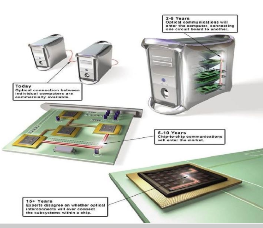
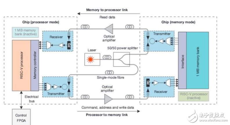
Silicon Photonics has captured the attention of both companies and researchers primarily due to its low cost and low power consumption. Silicon, as a material, is excellent for guiding light, making it a strong candidate for integrating optical components into semiconductor chips. As CMOS transistors continue to shrink in size, optical devices face physical limitations that prevent them from scaling down further, which has become a major area of research in recent years. Back in the 1980s and 1990s, pioneers who were concerned about the future of Moore’s Law began exploring alternatives to traditional silicon chips. They aimed to find a replacement once silicon reached its physical limits. I still remember my professor mentioning during my studies that the CMOS process would hit a wall when it reached a few dozen nanometers. However, today we have 7nm chips, and despite all the predictions, no large-scale alternative to CMOS has emerged yet. In this context, Silicon Photonics stands out as one of the most promising technologies under the "More than Moore" initiative. It represents an approach where optical components are integrated with electronic circuits on the same chip, opening up new possibilities for high-speed communication and data processing. The concept of integrated optics was first introduced by Bell Labs' S.E. Miller in 1969. With the advancement of microelectronics, the idea of combining optical and electrical devices on a single semiconductor substrate gained traction. By the 1990s, as silicon-based ICs became smaller, their feature sizes entered the optical communication wavelength range. The large refractive index difference between silicon (around 3.45) and silicon dioxide (around 1.44) made total internal reflection easier, which helped reduce the size of optical components and increase chip density. However, as CMOS transistors now reach around 10nm, optical components can't shrink further due to diffraction limits, which poses a challenge for continued miniaturization. As shown in the image above, we're currently at the stage of fiber-to-the-home and board-level interconnects in data centers. While 100G modules are becoming mature, widespread adoption of silicon photonics at the chip level is still a long way off. Interestingly, this article was published back in 2002, and even after 15 years, many of the predicted advancements haven’t fully materialized. Whether that's a good or bad thing remains to be seen. To summarize, the main appeal of Silicon Photonics lies in its low cost, low power consumption, and the suitability of silicon as a waveguide material. With the development of SOI technology, optical waveguide losses can be controlled at around 2–3 dB/cm. However, there are still several challenges that limit its broader application: How to integrate optoelectronic components: Light sources like lasers and photodetectors must be made using other materials such as III-V compounds or germanium, since silicon itself is an indirect bandgap material. This means that optical components cannot be fully fabricated on a standard CMOS process, leading to increased costs and complexity. How to control light: Controlling the wavelength and minimizing deviation is a big challenge. Small changes in fabrication parameters—like thickness or doping levels—can significantly affect optical performance. For example, a 10% shift in the thickness of a grating coupler can cause a 50nm shift in the coupling wavelength. Many optical modulators still require heaters for tuning, which adds to system complexity and cost. How to integrate with electronics: As CMOS transistors shrink, optical components face limitations due to diffraction and wavelength constraints. The integration of optical and electronic chips also requires advanced packaging techniques, which remain an active area of research. Here’s an example of a Silicon Photonics communication chip: Source: C. Sun et al., “Single-chip microprocessor of communicates directly using lightâ€, Nature, 2015. This paper presents a chip that could theoretically transmit data at 550 Gb/s. While the transmission wavelength isn’t in the industry-standard 1310nm or 1550nm range, the concept is straightforward: the electrical part handles signal processing (like SerDes and digital logic), while the optical part modulates the signal and sends it through fiber. At the receiving end, the optical signal is converted back into an electrical one. Some adjustment modules are needed at each step, but the overall idea is clear. In conclusion, I hope this brief introduction gives you a general understanding of Silicon Photonics. If you’re interested in learning more, feel free to reach out—I’d love to discuss and grow together in this exciting field. Telecom Battery Cabinet,Equipment Rack,Outdoor Electrical,Battery Cabinet Guangdong Yuqiu Intelligent Technology Co.,Ltd , https://www.cntcetltd.com