As an effective security precaution, the role of video surveillance is mainly concentrated in three aspects: one is early warning, which can analyze abnormal conditions and give an alarm; the second is real-time browsing, which can transmit real-time monitoring point images for users to browse; Event backtracking can store surveillance images and provide storage resources on demand. Among them, event backtracking is the most common and most important in current video surveillance applications, because in reality, users are more likely to track back the scene by playing back surveillance images after the event. Therefore, the effective storage of the surveillance point images is a very important part of the video surveillance system. Thanks to the continuous warming of network video surveillance construction in recent years, the storage market for video surveillance has also grown significantly. Analysys International analysis data shows that the market value of storage systems for video surveillance reached 470 million yuan in 2006, and in 2007, as operators, governments, and other industries accelerated the deployment of video surveillance, The market value of storage systems will reach 680 million yuan, with an annual growth rate of around 45%. Storage development in the field of video surveillance The development of storage in the field of video surveillance is closely related to the development of video surveillance itself. Video surveillance has experienced three stages: analog, digital, and network. Applications stored in the field of video surveillance have also experienced three stages: analog, digital, and network. Analog video surveillance originated in the 1980s. Image acquisition, transmission, and display are based on analog devices, and image storage is also based on analog devices, that is, video tape recorders (VCRs). Due to the use of video tapes, on the one hand, the storage capacity is greatly limited, on the other hand, image retrieval is very cumbersome, and remote calling cannot be achieved. In addition, there are obvious defects in terms of preservation time and system maintenance. In the late 1990s, digital video monitoring based on digital signal processing (DSP) gradually became popular, and various codec technologies have been widely used in image processing. The processed images can also be transmitted in the form of digital code streams. The storage has also begun to enter the digital era. The most typical application is a digital hard disk recorder (DVR), which uses an internal hard disk for image storage. This storage method has fundamental changes in storage time, image retrieval, system maintenance, and remote recall. However, because most of the digital video surveillance systems at this stage have obvious localization characteristics and relatively small scale, storage also shows obvious front-end and stand-alone characteristics. In recent years, with the rapid development of information network technology, networked video surveillance systems that are centrally managed and controlled through a central business platform, with network video servers and IP cameras as the front end, have begun to be widely deployed. Due to a reasonable architecture, flexible expansion, and clear layers, network video surveillance can bring users a new security application experience, thus quickly becoming the main form of building a new generation of video surveillance systems. The distributed front-end and platform architecture, centralized management and control, and flexible and convenient user access have made the storage part of the network video surveillance system begin to be networked. Networked storage brings a new storage architecture to video surveillance. On the one hand, users are more flexible in storage deployment and access is simpler. On the other hand, it is also more convenient to build a video surveillance system that requires mass storage.
We are manufacturing reliable Flex and Rigid-Flex boards using most advanced process. Rigid-flex PCBs improve reliability and lower costs associated with your device.
In electronics, we sometimes encounter seemingly new technologies that have roots in the past. Rigid Flex PCB technologies trace back approximately 50 years to the need to replace wiring harnesses in spacecraft. The first commercially available mobile computer (which weighed a little over 25 pounds!) used rigid flex technologies.
Firstly, the electronic engineer draws the circuit and outline of the flexible circuit board according to the requirement, and then sends it to the factory which can produce the flexible and rigid PCB. After the CAM engineer processes and plans the relevant documents, then arranges the FPC and PCB production lines needed for FPC production line to produce PCB. After the two kinds of flexible and rigid PCB are produced, the FPC and PCB are passed through according to the planning requirements of the electronic engineer. After seamless pressing and a series of details, the rigid flex PCB are finally made.
PCB is experienced in producing custom Rigid-Flex PCB, welcome your inquiry. Please check our Rigid Flex PCB manufacturing capabilities below.
Item
Manufacturing Capability
PCB Layers
1 - 12layers
Laminate
Flexible part: DuPont PI, Shengyi PI
Rigid part: PI/FR4
Maximum PCB Size(Length x Width)
406*610mm
Board Thickness
≤3.2mm
Finished board thickness tolerance
±2mil(±0.04m)
Copper Thickness
0.3oz - 1.0oz or higher
Min Tracing/Spacing
2.5mil/2.5mil
Min. Annular Ring
4mil
Min. Drilling Hole Diameter
8mil(0.2mm)
Min. hole size
8mil(0.2mm)
Min. finished via diameter
6mil(0.15mm)
Tolerance of dimension
3mil(0.076 mm)
Solder Mask Color
Green, White, Blue, Black, Red, Yellow
Silkscreen Color
White, Black, Yellow
Surface Finish
OSP
HASL(Hot Air Solder Leveling)
HASL Lead-Free
Flash Gold
ENIG (Electroless Nickle/Immersion Gold)
Immersion Tin
Immersion Silver
Special technologies
Impedance Control+/-10%
Gold fingers
Stiffener (PI/FR4)
Peelable solder mask
Another key issue in rigid flex reliability is the thickness and type of conductor found in the bend region. You can decrease thickness and mechanical stress by reducing the amount of plating on the conductors and using pads only plating. The use of heavy copper, gold, or nickel plating decreases flexibility at the bend and allows mechanical stress and fracturing to occur.
If you have assembly requirements for rigid flexible PCB, please refer to our PCB Assembly Service description.
Rigid Flex PCB Rigid Flex PCB,Flexible Printed Circuit Board,Polyimide PCB,FPC PCB JingHongYi PCB (HK) Co., Limited , https://www.pcbjhy.com
Rigid Flex PCB , combine the best of both Rigid PCB and flex circuits board into one unit
In order to let you have a deeper understanding of rigid Flexible PCB so as to select more suitable PCB products for your products, this article will give you a detailed understanding of the definition, type, application, manufacturing process, advantages, materials used in manufacturing, and stack up structure of rigid flexible PCB. And design guidelines
Rigid Flex PCB is an excellent combination of rigid boards and Flexible Circuits . Flex Rigid PCB is connected by PTH (plated through holes). Higher component density and better quality control can be guaranteed.
Today, laptop computers, wearable technologies, medical devices, test equipment, and satellites are a few of the applications that rely on rigid flex PCBs.
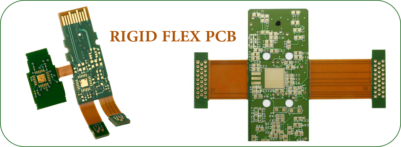
WHAT IS RIGID FLEX PCB?
Rigid Flex Printed Circuit Boards are boards using a combination of flexible and rigid board technologies in an application. Most rigid flex boards consist of multiple layers of flexible circuit substrates attached to one or more rigid boards externally and/or internally, depending upon the design of the application. The flexible substrates are designed to be in a constant state of flex and are usually formed into the flexed curve during manufacturing or installation.
Rigid Flex designs are more challenging than the design of a typical rigid board environment, as these boards are designed in a 3D space, which also offers greater spatial efficiency. By being able to design in three dimensions rigid flex designers can twist, fold and roll the flexible board substrates to achieve their desired shape for the final application's package.
As with conventional PCBs, you can mount components on both sides of the rigid board. Because of the integration that occurs between rigid and flex circuits, a rigid flex design does not use connectors or connecting cables between the sections. Instead, the flex circuits electrically connect the system together.
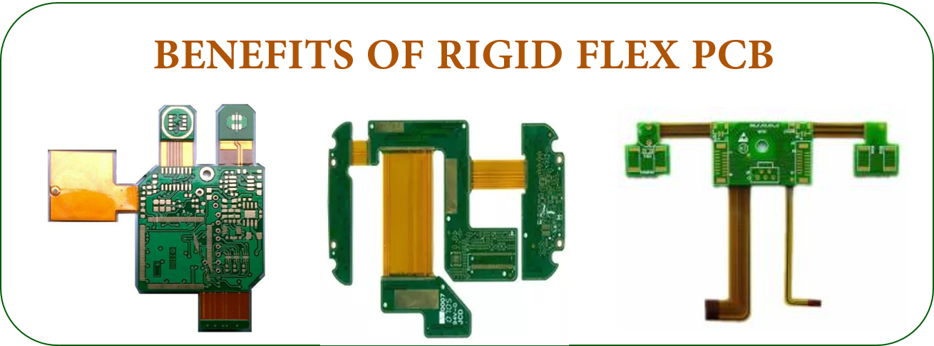
The lack of connectors and connecting cables accomplishes several things:
Every rigid flex PCB is divided into zones that feature different materials and varying layer counts. Rigid zones may have more layers than flexible zones, and materials shift from FR 4 to polyimide in transition zones.
TYPES OF RIGID FLEX PCB
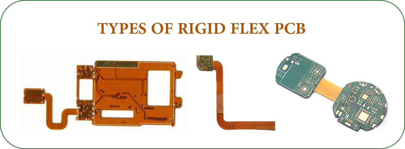
A four layer combination rigid flex circuit has four conductive copper layers. Typically, a four layer has two flexible layers and two rigid layers.
A 6 layer combination rigid flex circuit has six conductive copper layers. The two most common design types are as follows:
Rigid flex circuits combine the best of both rigid boards and flex circuits integrated together into one circuit. The two in one circuit is interconnected through plated thru holes. Rigid flex circuits provide higher component density and better quality control. Designs are rigid where extra support is needed and flexible around corners and areas requiring extra space.
RIGID FLEX PCB APPLICATIONS
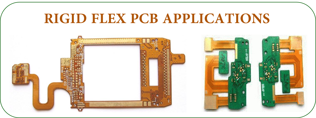
In consumer products, Rigid Flex doesn't just maximize space and weight but greatly improves reliability, eliminating many needs for solder joints and delicate, fragile wiring that are prone to connection issues. These are just some examples, but Rigid Flex PCBs can be used to benefit nearly all advanced electrical applications including testing equipment, tools and automobiles.
RIGID FLEX PCB Manufacturing
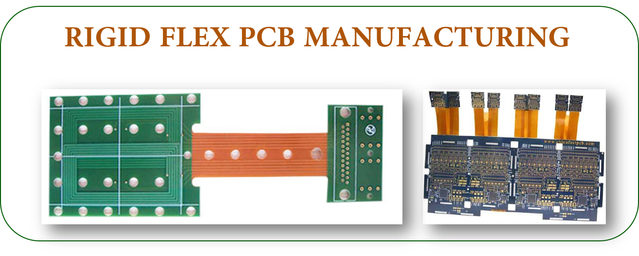
Because Rigid flex PCB is the combination of flexible PCB and rigid PCB, the production of Rigid-flex PCB should have both FPC production equipment and Rigid PCB production equipment.
RIGID FLEX PCB FABRICATION PROCESS
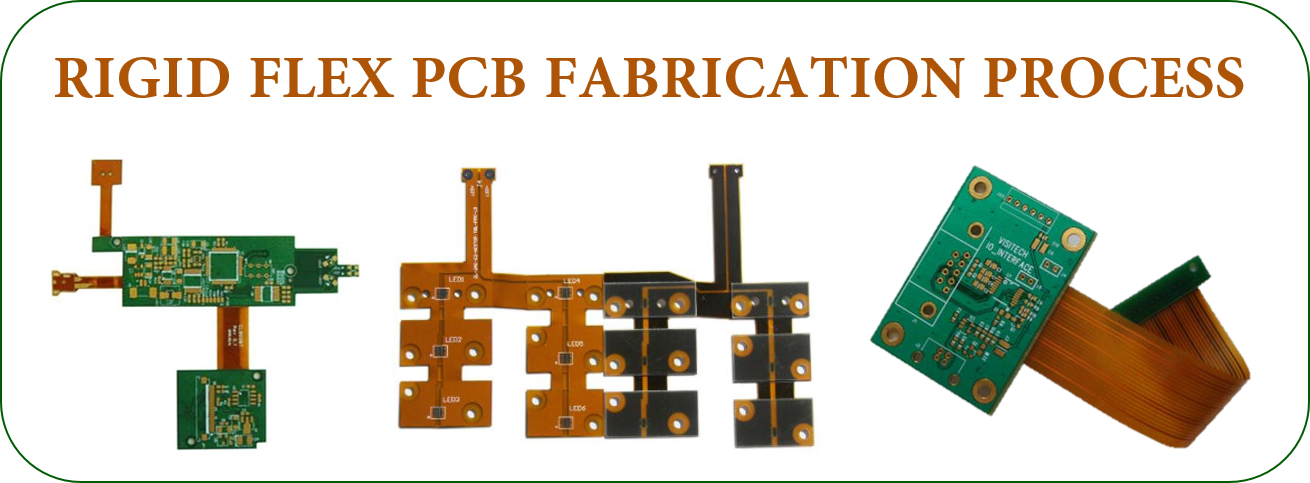
A very important link is that the rigid flex PCB is very difficult and has many details. Before shipment, it is generally necessary to carry out a full inspection, because of its high value, so as to avoid the loss of related interests caused by both suppliers and demanders.
BENEFITS OF RIGID FLEX PCB
RIGID FLEX PCB FABRICATION MATERIALS
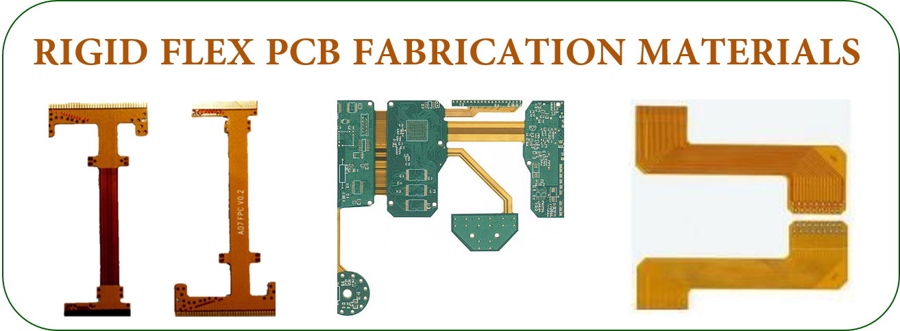
As the Rigid flex circuit market continues to expand, there have been many advances in technology including:
RIGID FLEX PCB DESIGN GUIDE
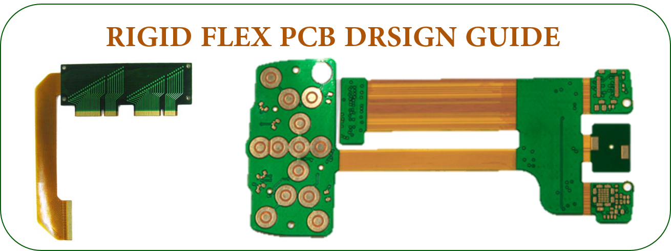
Different challenges offset the versatility and flexibility that allow you to build three dimensional designs and products. Traditional rigid flex PCB designs allowed you to mount components, connectors, and the chassis for your product to the physically stronger rigid part of the assembly. Again, in terms of traditional designs, the flexible circuit only served as an interconnect while lowering the mass and improving the resistance to vibration.
New product designs coupled with improved flex circuit technologies have introduced new design rules for rigid flex PCBs. Your design team now has the freedom to place components on the flexible circuit area. Combining this freedom with a multilayer approach to rigid flex design allows you and your team to build more circuitry into the design. However, gaining this freedom adds a few challenges in terms of routing and holes.
Flexible circuits always have bend lines that affect routing. Because of the potential for material stress, you cannot place components or vias close to the bend line.
And even when components are properly located, bending flex circuits places repeated mechanical stresses on surface mount pads and through holes. Your team can reduce those stresses by using through hole plating and by bolstering pad support with additional coverlay to anchor the pads.
As you design your trace routing, follow practices that reduce stress on your circuits. Use hatched polygons to maintain flexibility when carrying a power or ground plane on your flex circuit. You should use curved traces rather than 90° or 45° angles and use teardrop patterns to change trace widths.
These practices decrease stress points and weak spots. Another best practice distributes stress across traces by staggering the top and bottom traces for double sided flex circuits. Offsetting the traces prevents the traces from laying over each other in the same direction and strengthens the PCB.
You should also route traces perpendicular to the bend line to reduce stress. When moving from rigid to flex and back to rigid, the number of layers from one medium to the other may differ. You can use trace routing to add stiffness to the flex circuit by offsetting the routing for adjacent layers.
Electromechanical Factors Influence Design
When you design rigid flex PCBs, think in terms of electromechanical factors that affect both the flex circuit and the rigid board. As you build your design, focus on the ratio of bend radius to thickness. With flex circuits, tight bends or an increased thickness at the bend area increase the chances for failure. Fabricators recommend keeping the bend radius at a minimum of ten times the thickness of the flex circuit material and building a [paper doll" of the circuit to determine where bends occur.
You should avoid stretching the flex circuit along its outer bend or compressing it along the inner bend. Increasing the bend angle beyond 90° increases stretching at one point and compression at another point on the flex circuit.
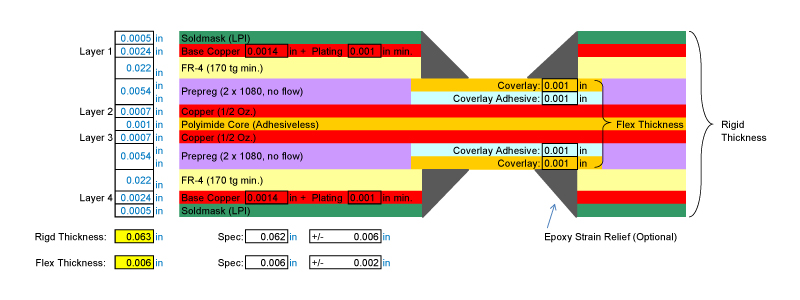
Rigid flex PCB stack up
Rigid Flex PCB assembly
YOU MAY ASK:
What is HDI PCB ?
HDI PCB is defined as a PCB with a higher wiring density per unit area than conventional PCB. They have finer lines and spaces, smaller vias and capture pads and higher connection pad density than employed in conventional PCB technology.
What is Metal Core PCB ?
MCPCB, Metal Core PCB, thermal PCB. Metal core pcb is abbreviated as MCPCB, it is made of thermal insulating layer, metal plate and metal copper foil, which has special magnetic conductivity, excellent heat dissipation, high mechanical strength and good processing performance.
What is MCPCB?
A Metal Core Printed Circuit Board (MCPCB) is a type of printed circuit board that contains a base metal material. The core is designed to redirect heat away from components which produce a substantial amount of heat.
Helpful Resources