introduction Low-noise amplifier (LNA) is a key circuit in wireless communication equipment. It is located at the forefront of the receiving equipment and amplifies the weak RF signal received from the antenna. Its noise performance and gain have an important impact on the performance of the whole machine. The circuit has the highest possible gain when it is smaller than the required noise index. In general, the minimum noise figure and maximum gain cannot be achieved at the same time, and their specifications are mainly determined by the input matching circuit. In order to meet the design requirements, the principle of giving due consideration is generally adopted. In the domestic GSM system, the operating frequency covers the range of l710MHz ~ 1990MHz. If a narrow-band LNA circuit is used, it can only be used for one system, and the application is limited. The wideband LNA circuit designed in this paper, whose operating frequency covers the above frequency range, makes the LNA circuit at the front end of the receiver very flexible. 1 Design simulation and optimization of low-noise amplifier circuit 1.1 Performance indicators and device selection The design requires that the operating frequency is 1700MHz to 2000MHz, the noise figure is less than 1.8dB, the gain is greater than 13dB, the input voltage standing wave ratio is less than 2.0, and the output voltage standing wave ratio is less than 3.5. The design uses AT41486 tube from Agilent. The device is a general-purpose NPN bipolar silicon tube with excellent characteristics such as low noise, high gain, and good frequency characteristics. The model uses the pb parameter model that comes with ADS. 1.2 Circuit stability Circuit stability is not only an important indicator of the amplifier circuit, but also a prerequisite for the normal operation of the circuit. The stable operation of the circuit is the most basic requirement, and any RF circuit has the possibility of oscillation in certain frequency bands and certain terminal conditions. There are many factors that cause circuit instability, mainly including the S parameter of the tube, the input and output matching circuit, and the selected operating point. Stability metrics are usually represented by stability factors K, B, and â–³, which are functions of the small-signal S-parameters of the device. When using the ADS tool, it is very convenient to calculate the two parameters K and B. Therefore, they are used here to measure the stability of the circuit. Calculated as follows: The stability factor of transistor AT41486 is simulated by ADS, and the results are shown in Table 1. 1.3 Noise figure The noise figure of the radio frequency system is related to the noise figure F of each stage circuit and the power gain G except the final stage. If the radio frequency system includes an N-level circuit, where the power gain of the i-th level is Gi and the noise figure is Fi, then the noise figure F of the radio frequency system can be expressed as: Closed Tricycle Electric Vehicle Three-Wheel Electric,Enclosed Electric Vehicle,Three-Wheeled Electric Vehicle,Closed Tricycle Electric Vehicle Jinan Huajiang environmental protection and energy saving Technology Co., Ltd , https://www.hjnewenergy.com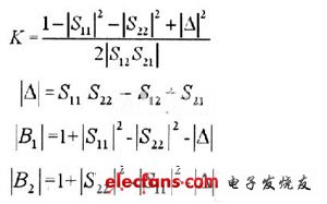
As long as K> l, | B |> 0, the circuit can work stably 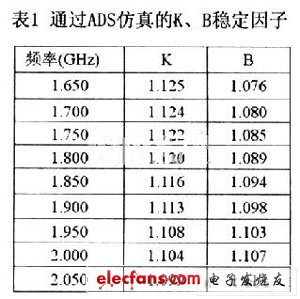
It can be seen from Table 1 that in the range of 1600MHz to 2100MHz, the requirements of K> 1 and B> 0 are met, indicating that the transistor is absolutely stable in the frequency band in which it operates, and no stabilization measures are required. 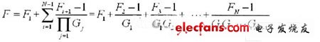
It can be seen from equation (5) that the noise figure F1 and gain G1 of the first stage have the greatest influence on the overall noise index of the circuit, and the LNA is exactly the first stage of the system. Therefore, its design is very important and requires a sufficiently small noise figure , As high gain as possible. For a single-stage LNA circuit, the noise figure can be calculated by the following formula (6), 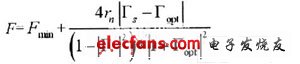
Among them, it represents the minimum noise figure of the transistor, the best source reflection coefficient when obtaining the minimum noise figure, and the equivalent noise resistance of the transistor, which are determined by the characteristics of the tube itself, and their values ​​are shown in Table 2. Is the source reflection coefficient at the input. It can be seen from equation (6) that at that time, the noise factor F of the amplifier circuit was the smallest, which was equal to Fmin. 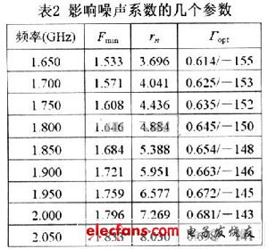
Since the gain Ggain of the amplifier circuit must be taken into account, the actual matching can be appropriately deviated in order to meet the requirements of the noise figure F in order to obtain a larger gain and meet the overall performance index. It can be seen from Table 2 that, as long as the design is reasonable, the noise figure of less than 1.8dB can be achieved in the range of 1700MHz ~ 2000MHz. When designing, input matching initial selection, and then optimize according to other indicators.