Small antenna for 300MHz to 450MHz transmitter Abstract: This application note details the various antennas used in handheld transmitters such as remote wireless key entry (RKE), tire pressure detectors (TPM), garage door openers, home security sensors, and TV remote controls. It also discusses loop / whip antennas, dielectric / "paper clip antennas", conventional whip antennas, helical antennas and patch antennas, and introduces the matching networks of these antennas and Maxim transmitters. Transmitters for remote wireless key entry (PKE), tire pressure detectors (TPM), garage door openers, home security sensors, and TV remote controls require small package antennas. Therefore, the antennas in almost all these applications are very short (ie, the size is one-tenth of the wavelength or even shorter). This application note describes the composition of these antennas and gives an assessment of the relevant impedance. A printed circuit board loop or whip antenna refers to a circular, elliptical, square, or rectangular lead made on a printed circuit board (PCB). If the design uses a double-layer PCB, the other side of the PCB layer where the antenna is located needs to be exposed. No ground plane or other leads should be placed under the antenna. A convex antenna or "paper clip" antenna, as shown in Figure 2, is very similar to a printed loop, whip antenna. It is usually an external wire or a flat metal strip that is connected to the PCB, adds a few millimeters of thickness, and has the outline of a printed antenna. The advantage of this structure is that the antenna is slightly away from other components of the PCB. The distal end of the antenna is suspended by an insulating bracket, or bent and connected to the PCB. When placed on the PCB, it can be connected to the pad, which can usually be connected to the ground plane, remain disconnected, or grounded through a passive device (such as an inductor or capacitor). Some handheld devices have enough space in a certain direction to place traditional whip antennas or "broken" antennas. It is usually a 2cm to 5cm wire, sometimes covered with protective dielectric material. This kind of antenna can choose the existing (OTS) antenna on the market to provide specific performance specifications, or it can be made by metal sheet (DIY). The impedance of the OTS antenna has better repeatability than other PCB antennas, which may be due to the antenna's greater internal losses, which make its resistance larger. Some large-size OTS antennas may have an impedance close to 50Ω and no reactance (capacitive or inductive). Usually, an internal inductance is used to cancel the capacitive load. Figure 3 shows two independent whip antennas. A helical antenna is much like a thicker whip antenna, usually a thin coil with a length of 2cm to 5cm. Figure 4 shows a corresponding example. Many users wind their own coils. There are also many products on the market for helical antennas. Most helical antennas have 20Ω to 50Ω resistance and 0Ω imaginary impedance (that is, there is no capacitive or inductive impedance). In theory, the coil inductance cancels the whip antenna Of the capacitor. The spiral antenna is easy to match, but its radiation intensity will not be better than that of other antennas. Chip antennas are rarely used in 300MHz to 450MHz systems because the conventional size of these antennas is a quarter of the wavelength. Unlike other PCB antennas, chip antennas have a ground plane on another PCB. The impedance of the small chip antenna is very close to the impedance of the whip antenna, because the non-driven end of the antenna is open, forming a capacitor. The impedance of a small chip antenna is equivalent to a 1pF to 5pF capacitor in series with a small resistor. Figure 5 shows a good matching network for matching the Maxim transmitter with any of the above antennas. Specific pads can be composed of inductors and capacitors, depending on the type of antenna required. Series elements (E6) or parallel elements (E5) are used to cancel some or all of the reactance and change the equivalent resistance of the antenna. Components E3, E4 and E5 are usually used to form a π-type network low-pass filter (LPF) to suppress the higher harmonics of the PA output. If E5 is used as a tuning device for the antenna, its value can be integrated into the π-type network low-pass filter. The inductance (L1) is used to isolate RF interference from the DC power supply, and the capacitor (C1) is a DC blocking capacitor. When necessary, an appropriate value can be selected to achieve other impedance transformations. When driving resistance (actual resistance) from 125Ω to 250Ω, most of Maxim's transmitters can provide the best efficiency and power output. The only exception is the high-power MAX7044, which works best when the resistance is between 60Ω and 120Ω. It can maintain the voltage swing of the RF signal when the load impedance is small. Strong Suction Vacuum Cleaner,Strong Suction Robot Vacuum Cleaner,Strong Suction Wired Vacuum Cleaner,High Power Vacuum Cleaner NingBo CaiNiao Intelligent Technology Co., LTD , https://www.intelligentnewbot.com
The "drive" or "feed point" of the antenna lead is the input—connected directly or through a matching network to the power amplifier (PA). The matching network components are placed on another layer of the PCB, above the ground layer. Usually on the drive side, the ground layer is on another PCB layer, so the printed antenna area is bare. The other end of the printed antenna is connected to the ground layer, usually through a large copper area at the top terminal of the PCB and connected to ground through many vias.
If the other end of the antenna is disconnected, the antenna becomes a whip antenna, or a monopole antenna. The whip antenna can be realized by PCB wiring, which can be straight or semicircular, elliptical, square or rectangular. Figure 1 shows a schematic diagram of a PCB loop / whip antenna. 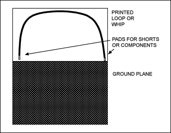
Figure 1. PCB loop or whip antenna
A multi-functional antenna is loop-shaped and will not be short-circuited directly to the ground. Its end is a pad / wire, which can be disconnected or shorted to ground. This pad usually has an inductance or capacitance to tune the antenna to the appropriate frequency.
The small loop antenna has the typical size of a handheld transmitter (each side is 2cm to 5cm), with an inductance of 30nH to 100nH and an equivalent series resistance of a few Ω. Theoretically, the series resistance is less than 1Ω, but on-board losses, dielectric losses, coupling losses of other circuit components, and measurement errors may cause the resistance to be as high as 10Ω when measured with a network analyzer.
A typical size whip antenna in a handheld transmitter has a capacitance of 1pF to 5pF and an equivalent series resistance of a few Ω. In theory, the equivalent series resistance of the small whip antenna is 10 times the equivalent resistance of a loop antenna of the same size, but it is still very small, and the actual measured resistance value is the same as the resistance of the loop antenna.
Although printed antennas save money, the disadvantage is that the antenna characteristics depend on the tolerances of the plate and the leads themselves. Some surface-mount antennas have good repeatability. When the consistency of the antenna is high, this method should be considered. 
Figure 2. Convex antenna
The impedance of the convex antenna is the same as the impedance of the printed antenna. 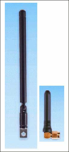
Figure 3. Independent whip antenna (picture does not include antenna parameters) 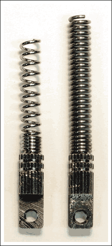
Figure 4. Helical antenna (picture does not include antenna parameters) 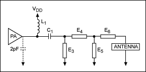
Figure 5. Transmitter's universal matching network, including ring, whip, spiral or other commonly used antennas
Figure 6 shows the matching network of a small PCB loop antenna. Choose a series capacitor (C4) to cancel most (not all) loop inductance. This inductance converts the small series resistance into inductive impedance. 
Figure 6. Recommended matching network for PCB loop antennas