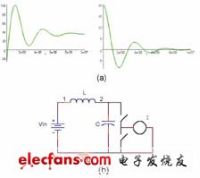
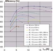
introduction As the computer industry moves toward DC-DC converters that can deliver up to 200A at 1V, PCB layout technology needs to meet the requirements of this challenging new converter. In order to compare the effects of various wiring defects, we focus on the effects of parasitic inductance in the circuit, especially those related to the source, drain, and gate of the switching MOSFET. We built a PCB for testing a DC-DC converter that can input 12V DC and convert it to 1.3V with an output current of up to 20A. We use a plug-in board to assemble and change the inductance at each MOSFET electrode separately or simultaneously (Figure 1). We chose to use the inductance value as a percentage of the total inductance of a specially designed 2-inch board, rather than the actual value, because the wiring personnel only know the length of a particular trace and do not necessarily know the value of its inductance. Test design We use converter efficiency to measure the effects of these parasitic inductances. This is because efficiency is a standard indicator of the performance of a DC-DC converter. The test is divided into the following sections: The scaling factor of each inductance value of the MOSFET drain, source and gate is adjusted, and the effect on the synchronous rectifier is observed by measuring the conversion efficiency. Through the combination of any two of the above, to understand the relationship between them. The inductor test board has an inductance of 43nH and is typically set to 0%, 25%, 50%, and 100%. In our experiments, the parasitic resistance on the inductive test board has little effect and can be ignored. Since the detrimental effects of parasitic inductance are frequency dependent, we tested at three preset switching frequencies: 300kHz, 600kHz, and 1MHz. This way we can recognize the importance of designing the design from the normal switching frequency to the higher frequency in the future. Everyone knows that in power circuits, the length of all traces must be kept to a minimum to avoid voltage and current ringing, reduce overall EMI of the board, and avoid negative effects on "stable" components in the circuit (especially For analog control circuits and related components). In addition, the reference shows that the source inductance of the control MOSFET has a non-linear effect on the increase in source current fall time, resulting in greater power dissipation and lower conversion efficiency (see Figure 2). In Figure 2, CH1 is the gate-to-ground voltage of the high-side (HS) MOSFET M1. Ch2 is the source-ground voltage of the HS MOSFET M1 in the same figure. The calculated value of the M1 traces Ch1-Ch2 in Figure 2 represents the gate-source voltage of the HS MOSFET. Ch3 and Ch4 are the leakage currents of M2 and M1, respectively. In addition to the above phenomena, the source inductance also causes ringing at the switch node. The gate and drain inductances cause ringing on both electrodes and cause further losses. The loss associated with each cycle, P1, can be calculated as 1/2&TImes;I2&TImes;L&TImes;fs Where I is the current in the inductor; L is the parasitic inductance; fs is the switching frequency, at which point all of the energy stored in the parasitic inductor is dissipated during the ringing process (see Figure 3). Figure 3 depicts the oscillating current and voltage in a typical drain parasitic inductor. Note that the current and voltage waveforms tend to zero before the start of the next switching cycle. The energy stored in the inductor is converted to the heat of the associated parasitic resistance. Finally, for the case of two or more parallel MOSFETs, the imbalance of the source inductance causes an imbalance in the current distribution, which in turn results in greater losses and lower efficiency. Test circuit and circuit board The circuit used is a synchronous rectification topology that operates in an open loop. This is to rule out any effects that the control loop may have on circuit performance, and let us focus on the power conversion efficiency, especially the performance of the MOSFET. We know that there are severe ringing in high inductance conditions, especially at the switch node. The gate driver IC is chosen to withstand such ringing without adverse effects. The four-layer board uses two ounces of copper and the inner two layers are the ground plane and power plane. Pay attention to all the rules of good wiring when wiring. Effect of gate inductance Efficiency is a function of gate inductance and switching frequency. It can be seen from the figure: The gate inductance has little effect on efficiency at a switching frequency of 300 kHz. When the switching frequency is 600 kHz, the effect of the gate inductance is much more significant, and the efficiency is 1.2% at 20A. At 1 MHz, the deterioration of efficiency almost completely disappeared. We have not studied this reason, we can guess that the 50% probability is the factor of resonance to offset its loss. The resonance phenomenon of the MOSFET gate drive should be further studied. We observed that the gate inductance has little effect on the efficiency of the control and synchronous MOSFETs. Source inductance Source inductance has a more pronounced effect on efficiency. In some cases, we had to abort the test before reaching the maximum current because the MOSFET temperature was greater than 130 °C. Figure 5 shows the results of the research on the control MOSFET. Careful examination of these results shows that: At a frequency of 300 kHz and an inductance of 100%, the DC-DC converter cannot operate at 20A full current because the MOSFET temperature exceeds 130 °C. The same can be found at 50% inductance at 600 kHz and 1 MHz. It is observed that the deterioration of efficiency due to source inductance is more severe than in the case of no source inductance. When the inductance is 50% and the current is 15A, the efficiency is reduced by 7% even at the switching frequency of 300 kHz. When the inductance is 100%, the efficiency deteriorates to 11%. At 600kHz and 1MHz switching frequencies, the effect is more pronounced than in the absence of source inductance, and efficiency degradation is more severe (see Figure 5). Obviously, even the smallest source inductance will reduce efficiency, especially when the switching frequency is ≥600kHz.
The distribution box is a massive parameter on the data. Generally, it constitutes a low-voltage forest. According to the electrical wiring, it is required to assemble the switchgear, measuring instrument, protective electrical appliance and auxiliary equipment in a closed or semi-closed metal cabinet or on the screen to form a low-voltage power distribution. box. The circuit can be switched on or off with a manual or automatic switch during normal operation.
Our company's Distribution Boxes are mainly divided into six series(as follow),had exported into global market for many years:
Universal Junction Boxes
Distribution Boxes Distribution Boxes,Terminal Box,Switch Box,Control Switch Box Ningbo Bond Industrial Electric Co., Ltd. , https://www.bondelectro.com

Euro type Switch Boxes
Distribution Box
Locks for Switch Boxes
Industrial Plug and Socket
JXF Water Proof Metallic Panel Board

