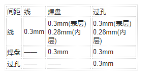
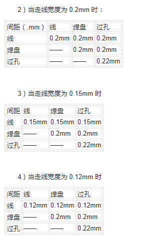
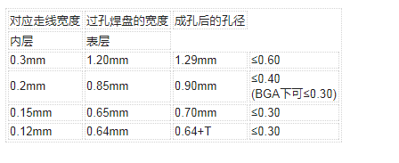
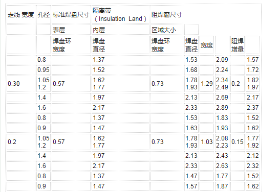
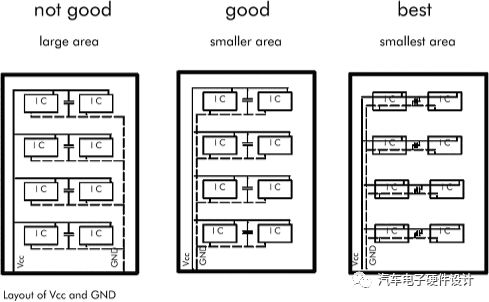
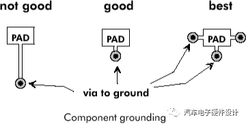
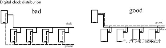
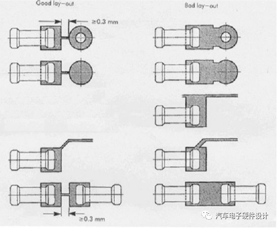
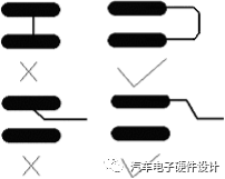
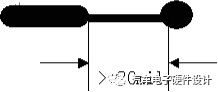
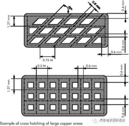
(I) Wiring design principles 1. Lines should avoid sharp corners and right angles. Use 45° alignment. 2. The adjacent signal lines are in orthogonal directions. 3. The high frequency signal is as short as possible. 4. The input and output signals should avoid adjacent parallel lines. It is better to add ground between lines to prevent feedback coupling. 5. The direction of the dual-panel power lines and ground lines is preferably the same as the data flow direction to enhance the anti-noise ability. 6. Digital ground and analog ground should be separated. For low-frequency circuits, the ground should be connected with a single point as much as possible; high-frequency circuits should be grounded with multiple points in series. For digital circuits, the ground should be closed into a loop to improve noise immunity. 7. For the clock line and the high-frequency signal line, the line width should be taken into account according to its characteristic impedance, so as to achieve impedance matching. 8. The wiring of the entire circuit board should be uniform and the hole should be punched to avoid obvious uneven density. When there is a large blank area in the signal of the outer layer of the printed circuit board, auxiliary lines should be added to make the distribution of metal lines on the surface of the board substantially balanced. (II) Process Requirements for Cabling Design 1. Usually we use the most commonly used trace width and via size when wiring: Note: The vias under the BGA package components need to be covered with solder masks on the front and back sides, depending on the process requirements. 1) When the trace width is 0.3mm It is worth noting that the space between the pads under the BGA and the via pads between the pads is also the line width. Due to the technical difficulty, it is not recommended to use 0.12mm line width. 5) When the line width is less than or equal to 0.12mm, the via pads need to add teardrops. T in the table represents the need to add teardrops. When the board size is greater than 600mm, the pad width of the vias needs to be increased by 0.1mm. Table unit: mm For non-pored holes, the solder resist window should be 0.50 mm larger than the hole diameter . The width of the surface isolation region is also determined by the size of the hole. When the diameter of the hole is 3.3mm or less, the range is “aperture +2.0â€; when the diameter of the hole is more than 3.3mm, the range is 1.6 times of the hole diameter . The inner isolation range is "Aperture +2.0mm" 2. Specific wiring principles: 1) Power and ground wiring Try to give a separate power layer and bottom layer; even if you want to pull in the surface, the power line and ground should be as short and thick enough. For multilayer boards, there are generally power layers and ground layers. It should be noted that only the analog and digital parts of the ground and power supply must be split even if the voltage is the same. For single and double-layer power cables should be as thick and short as possible. The width requirements of the power supply and ground lines can be calculated based on the maximum 1A line current of 1mm , and the loop formed by the power supply and ground is as small as possible. As shown below: In order to prevent a long power cable, power line noise is coupled directly to the load device, should each device before entering the first power supply decoupling. In order to prevent them from interfering with each other, the power of each load is independently de-interleaved, and filtering is performed before entering the load. As shown below: Keep good grounding in the wiring. As shown below: 2. Special signal line wiring A. Clock wiring: The clock line is one of the most important factors affecting EMC. In the clock line should be less holes, as far as possible to avoid and other signal lines and run the line, and should be away from the general signal line to avoid interference on the signal line. At the same time, avoid the power section on the board to prevent the power supply and the clock from interfering with each other. When using multiple clocks with different frequencies on one board, two clock lines with different frequencies cannot be paralleled. The clock line should also be avoided near the output interface as much as possible to prevent the high frequency clock from being coupled to the output cable and transmitting along the line. If there is a chip on the board that has a special clock, it should not be routed underneath it. It should be laid underneath it and, if necessary, it can be cut specially. For many chips have a reference crystal oscillator, these crystals should not be located below the line, to be copper isolation. At the same time, the crystal case can be grounded B. Pairs of differential signal lines Pairs of differential signal lines appear, generally parallel, with as few holes as possible. When holes must be punched, holes should be drilled together to achieve impedance matching. C. A set of buses with the same attributes should be aligned side by side as far as possible to achieve the same length. D. Some basic principles of routing. Considering heat dissipation and avoiding continuous welding, try to use Good lay-out as shown below to avoid Bad lay-out. When the distance between two solder joints is small (such as the pad adjacent to the patch device), the solder joints must not be directly connected. The via from the pad pad is as far away from the pad as possible. 3) Adding copper Multilayer copper plating inside, use negative. If the outer layer of copper is to be completely solidified, there should not be a gap, and it is best to use copper in the form of a grid. The grid must not be smaller than 0.6mm X 0.6mm. It is recommended to use 30mil X 30mil grid copper. Pictured Dc Solar Pump,Solar Centrifugal Pump,Surface Centrifugal Pump ,Dc Solar Water Pumps Wuxi Doton Power , http://www.dotonpower.com