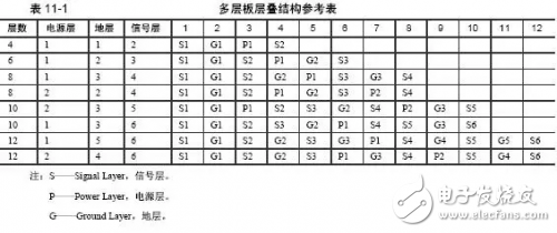
Before designing a multi-layer PCB circuit board, the designer needs to first determine the structure of the circuit board used according to the circuit size, circuit board size and electromagnetic compatibility (EMC) requirements, that is, decide whether to use 4, 6 or More layers of circuit board. After determining the number of layers, determine the placement of the internal electrical layers and how to distribute different signals on these layers. This is the choice of multilayer PCB stack structure. The stacked structure is an important factor that affects the EMC performance of the PCB board, and also an important means to suppress electromagnetic interference. This section will introduce the relevant content of the multilayer PCB laminate structure. 11.1.1 Selection of layers and superposition principle More factors need to be considered in determining the stack structure of a multilayer PCB board. In terms of wiring, the more layers, the better the wiring, but the cost and difficulty of the board will also increase. For manufacturers, whether the stacked structure is symmetrical or not is the focus of attention in the manufacture of PCB boards, so the selection of the number of layers needs to consider the needs of various aspects to achieve the best balance. For experienced designers, after completing the pre-layout of components, they will focus on the PCB bottleneck. Combine with other EDA tools to analyze the wiring density of the circuit board; then combine the number and type of signal lines with special wiring requirements such as differential lines and sensitive signal lines to determine the number of signal layers; then according to the type of power supply, isolation and anti-interference Requirements to determine the number of inner electrical layers. In this way, the number of layers of the entire circuit board is basically determined. After determining the number of layers of the circuit board, the next job is to arrange the order of the circuits of each layer in a reasonable manner. In this step, the main factors to be considered are the following two points. (1) Distribution of special signal layers. (2) Distribution of power and ground layers. If the number of layers of the circuit board is more, there are more types of arrangement and combination of special signal layers, ground layers and power layers. It is also more difficult to determine which combination method is optimal, but the general principles are as follows. (1) The signal layer should be adjacent to an internal electrical layer (internal power / ground layer), and use the large copper film of the internal electrical layer to provide shielding for the signal layer. (2) The internal power layer and the ground layer should be tightly coupled, that is to say, the thickness of the medium between the internal power layer and the ground layer should take a small value to increase the capacitance between the power layer and the ground layer and increase the resonance frequency . The thickness of the medium between the internal power layer and the ground layer can be set in Protel's Layer Stack Manager. Select the [Design] / [Layer Stack Manager ...] command, the system pops up the layer stack manager dialog box, double-click the Prepreg text with the mouse, a dialog box as shown in Figure 11-1 pops up, and the insulation can be changed in the Thickness option of the dialog box The thickness of the layer. If the potential difference between the power supply and the ground wire is not large, you can use a smaller thickness of the insulating layer, such as 5mil (0.127mm). (3) The high-speed signal transmission layer in the circuit should be the signal intermediate layer and be sandwiched between the two inner electrical layers. In this way, the copper films of the two inner electrical layers can provide electromagnetic shielding for high-speed signal transmission, and can also effectively limit the high-speed signal radiation between the two inner electrical layers without causing interference to the outside. (4) Avoid two signal layers directly adjacent. Crosstalk is easily introduced between adjacent signal layers, resulting in circuit failure. Adding a ground plane between the two signal layers can effectively avoid crosstalk. (5) Multiple grounded inner electrical layers can effectively reduce the grounding impedance. For example, the A signal layer and the B signal layer use separate ground planes, which can effectively reduce common mode interference. (6) Take into account the symmetry of the layer structure. 11.1.2 Commonly used stacked structures The following uses an example of a 4-layer board to explain how to optimize the arrangement and combination of various stacked structures. For commonly used 4-layer boards, there are the following stacking methods (from the top layer to the bottom layer). Obviously, Scheme 3 lacks effective coupling between the power and ground layers and should not be used. So how should options 1 and 2 be selected? In general, designers will choose option 1 as the structure of the 4-layer board. The reason for the selection is not that Option 2 cannot be adopted, but the general PCB boards only place components on the top layer, so Option 1 is more appropriate. However, when components need to be placed on both the top layer and the bottom layer, and the dielectric thickness between the internal power layer and the ground layer is large, and the coupling is not good, you need to consider which layer has fewer signal lines. For Option 1, there are few signal lines on the bottom layer, and a large area of ​​copper film can be used to couple with the POWER layer; on the contrary, if the components are mainly arranged on the bottom layer, Option 2 should be used to make the board. If the stacked structure shown in Figure 11-1 is used, the power layer and the ground layer are already coupled. Considering the symmetry requirements, scheme 1 is generally adopted. After the analysis of the laminated structure of the 4-layer board is completed, the arrangement and combination method and the preferred method of the laminated structure of the 6-layer board are explained by an example of the combination method of the 6-layer board. (1) Siganl_1 (Top), GND (Inner_1), Siganl_2 (Inner_2), Siganl_3 (Inner_3), POWER (Inner_4), Siganl_4 (Bottom). Option 1 uses a 4-layer signal layer and a 2-layer internal power / ground layer, with more signal layers, which is conducive to the wiring work between components, but the shortcomings of this program are also obvious, manifested in the following two aspects. â‘ The power layer and ground layer are far apart and not fully coupled. Compared with Option 1, Option 2 has sufficient coupling between the power layer and the ground layer, which has certain advantages over Option 1. However, Siganl_1 (Top) and Siganl_2 (Inner_1) and Siganl_3 (Inner_4) and Siganl_4 (Bottom) signal layers are directly Adjacent, the signal isolation is not good, and the problem of crosstalk is not solved. (3) Siganl_1 (Top), GND (Inner_1), Siganl_2 (Inner_2), POWER (Inner_3), GND (Inner_4), Siganl_3 (Bottom). Compared with Option 1 and Option 2, Option 3 reduces a signal layer and adds an internal electrical layer. Although the number of layers available for wiring is reduced, this option solves the common defects of Option 1 and Option 2. â‘ The power layer and ground layer are tightly coupled. Taking all aspects into consideration, Scheme 3 is obviously the most optimized one. At the same time, Scheme 3 is also a layered structure commonly used for 6-layer boards. The layer design of the circuit board is closely related to the characteristics of the actual circuit. The anti-interference performance and design focus of different circuits are different, so in fact these principles do not have a determined priority for reference. But what can be determined is that the design principle 2 (the internal power layer and the ground layer should be tightly coupled) needs to be satisfied first in the design. In addition, if the circuit needs to transmit high-speed signals, then the design principle 3 (high-speed signal transmission layer in the circuit It should be the middle layer of the signal, and sandwiched between the two inner layers) must be satisfied. Table 11-1 gives the reference scheme of the multilayer board stacking structure for readers' reference. 11.2.1 General principles of component layout The general principles designers need to follow during the circuit board layout process are as follows. (1) Components are best placed on one side. If you need to place components on both sides, placing pin-type components on the bottom layer (Bottom Layer) may cause the circuit board to be difficult to place and not conducive to soldering, so it is best to place only chip components on the bottom layer (Bottom Layer) , Similar to the common component layout method on the computer graphics PCB board. When placed on one side, it is only necessary to make a screen printing layer on one side of the circuit board, which is convenient for reducing costs. (2) Reasonably arrange the position and direction of interface components. Generally speaking, as the connector components connecting the circuit board and the outside world (power supply, signal line), they are usually arranged on the edge of the circuit board, such as serial port and parallel port. If it is placed in the center of the circuit board, it is obviously not conducive to wiring, and it may not be connected due to the obstruction of other components. In addition, pay attention to the direction of the interface when placing the interface, so that the connection cable can be led out smoothly, away from the circuit board. After the interface is placed, the type of the interface should be clearly marked with the String of interface components; for the power interface, the voltage level should be marked to prevent the circuit board from being burned due to incorrect wiring. (3) It is better to have a wide electrical isolation zone between high-voltage components and low-voltage components. In other words, do not put components with very different voltage levels together, which is not only conducive to electrical insulation, but also has great benefits for signal isolation and anti-interference. (4) Components with close electrical connections are best placed together. This is the modular layout idea. (5) For components that are prone to noise, such as high-frequency devices such as clock generators and crystal oscillators, they should be placed as close to the clock input of the CPU as possible. High-current circuits and switching circuits are also prone to noise. These components or modules should also be kept away from high-speed signal circuits such as logic control circuits and storage circuits during layout. To connect to improve the overall anti-interference ability and working reliability of the circuit board. (6) Place decoupling capacitors and filter capacitors around the power supply and the chip as much as possible. The arrangement of decoupling capacitor and filter capacitor is an important measure to improve the power quality of the circuit board and the anti-interference ability. In practical applications, the traces, pin connections and wiring of the printed circuit board may bring a large parasitic inductance, resulting in high-frequency ripples and glitches in the power supply waveform and signal waveform. Place a 0.1ïF decoupling capacitor between them to effectively filter out these high-frequency ripples and glitches. If a chip capacitor is used on the circuit board, the chip capacitor should be placed close to the power supply pin of the component. For the power conversion chip or the power input terminal, it is better to arrange a 10ïF or larger capacitor to further improve the power quality. 11.2.2 General principles of component wiring The general principles that designers need to follow in the circuit board wiring process are as follows. (1) The setting principle of the spacing between printed traces of components. The spacing constraints between different networks are determined by factors such as electrical insulation, manufacturing process, and component size. For example, the pin spacing of a chip component is 8mil, the [Clearance Constraint] of the chip can not be set to 10mil, the designer needs to set a 6mil design rule for the chip separately. At the same time, the setting of the distance must also take into account the production capacity of the manufacturer. In addition, an important factor that affects components is electrical insulation. If the potential difference between two components or the network is large, electrical insulation needs to be considered. The gap safety voltage in a general environment is 200V / mm, which is 5.08V / mil. Therefore, when there are both high-voltage circuits and low-voltage circuits on the same circuit board, special attention must be paid to sufficient safety distance. (2) The choice of the routing of the corner of the line. In order to make the circuit board easy to manufacture and beautiful, the corner mode of the line needs to be set during the design, and 45 °, 90 ° and arc can be selected. Generally, sharp corners are not used. It is better to use arc transition or 45 ° transition, and avoid 90 ° or more sharp corner transition. The connection between the wire and the pad should also be as smooth as possible to avoid the appearance of small pointed feet, which can be solved by using teardrops. When the center distance between the pads is less than the outer diameter D of a pad, the width of the wire can be the same as the diameter of the pad; if the center distance between the pads is greater than D, the width of the wire should not be greater than the pad diameter. When the wire passes between the two pads and is not connected to it, the maximum and equal spacing should be maintained with them. Similarly, the spacing between the wire and the wire should also be uniform and equal to maintain the maximum. (3) How to determine the width of the printed trace. The width of the trace is determined by the current level and anti-interference of the wire. The larger the current, the wider the trace. Generally, the power line should be wider than the signal line. In order to ensure the stability of the ground potential (less affected by the change of the ground current), the ground wire should also be wider. Experiments show that when the thickness of the copper film of the printed wire is 0.05mm, the current carrying capacity of the printed wire can be calculated according to 20A / mm2, that is, 0.05mm thick and 1mm wide wire can flow 1A of current. Therefore, for general signal lines, the width of 10-30 mils can meet the requirements; the line width of high-voltage, high-current signal lines is greater than or equal to 40 mils, and the spacing between the lines is greater than 30 mils. In order to ensure the anti-stripping strength and working reliability of the wire, as far as the board area and density allow, the widest wire should be used to reduce the line impedance and improve the anti-interference performance. For the width of the power line and the ground line, in order to ensure the stability of the waveform, as far as the wiring space of the circuit board allows, try to make it thicker. Generally, at least 50mil is required. (4) Anti-interference and electromagnetic shielding of printed wires. The interference on the conductor mainly includes the interference introduced between the conductors, the interference introduced by the power cord and the crosstalk between the signal lines, etc. Reasonable arrangement and arrangement of wiring and grounding methods can effectively reduce the source of interference and make the designed circuit board more Good electromagnetic compatibility performance. For high-frequency or other important signal lines, such as clock signal lines, on the one hand, the traces should be as wide as possible, on the other hand, they can be isolated from the surrounding signal lines in the form of a ground (that is, a closed ground The cable "wraps" the signal line, which is equivalent to adding a layer of ground shield. The analog and digital grounds must be wired separately and cannot be mixed. If the analog ground and digital ground need to be unified into one potential at the end, one point grounding method should usually be adopted, that is, only one point is selected to connect the analog ground and digital ground to prevent the formation of a ground loop and cause a ground potential shift. After the wiring is completed, a large area of ​​ground copper film, also known as copper, should be applied on the top and bottom where no wires are laid, to effectively reduce the impedance of the ground wire, thereby weakening the high-frequency signal in the ground wire, and at the same time Area grounding can suppress electromagnetic interference. A via in the circuit board will bring about 10pF of parasitic capacitance, which is especially harmful for high-speed circuits; at the same time, too many vias will also reduce the mechanical strength of the circuit board. Therefore, when wiring, the number of vias should be reduced as much as possible. In addition, when using penetrating vias (through holes), pads are usually used instead. This is because when the circuit board is manufactured, it is possible that some through-type vias (through holes) are not penetrated due to processing reasons, and the pads can certainly be penetrated during processing, which is equivalent to giving Production brings convenience. The above is the general principle of PCB board layout and wiring, but in actual operation, the layout and wiring of components is still a very flexible work, the layout and wiring of components are not unique, and the results of layout and wiring are very To a large extent still depends on the experience and ideas of the designer. It can be said that there is no standard to judge the right and wrong of the layout and wiring scheme, and only the relative advantages and disadvantages can be compared. Therefore, the above layout and wiring principles are only for design reference, and practice is the only criterion for judging the pros and cons.
Heavy Duty Connectors (HDC) provide extensive industrial inserts,
alternate or direct-current connectors for heavy-duty industrial applications; multi-pole connectors for use in electronic machinery, robots, electric panels, control equipment, power and control- or signal-circuit connectivity; enclosures for standard, harsh and EMC environments; plastic and metal cable glands. All products are designed with top-quality materials.
The principal HDC parts are comprised of die-cast aluminum alloy with either a polyester powder (nickel-plated for EMC versions) finish or a self-extinguishing thermoplastic. Coupling stability and accidental opening protection is achieved by two locking systems (mono-block levers in galvanized or stainless steel or springs and pegs in stainless steel). Sealing of dust, water and aggressive agents is assured with internal protective gaskets.
Heavy duty connector Wonke Electric CO.,Ltd. , https://www.wkdq-electric.com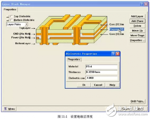
(1) Siganl_1 (Top), GND (Inner_1), POWER (Inner_2), Siganl_2 (Bottom).
(2) Siganl_1 (Top), POWER (Inner_1), GND (Inner_2), Siganl_2 (Bottom).
(3) POWER (Top), Siganl_1 (Inner_1), GND (Inner_2), Siganl_2 (Bottom).
â‘¡ The signal layers Siganl_2 (Inner_2) and Siganl_3 (Inner_3) are directly adjacent to each other, the signal isolation is not good, and crosstalk is easy to occur.
(2) Siganl_1 (Top), Siganl_2 (Inner_1), POWER (Inner_2), GND (Inner_3), Siganl_3 (Inner_4), Siganl_4 (Bottom).
â‘¡ Each signal layer is directly adjacent to the inner electrical layer and is effectively isolated from other signal layers, making crosstalk less likely.
â‘¢ Siganl_2 (Inner_2) is adjacent to the two inner electrical layers GND (Inner_1) and POWER (Inner_3), which can be used to transmit high-speed signals. The two inner electric layers can effectively shield the outside interference to the Siganl_2 (Inner_2) layer and Siganl_2 (Inner_2) to the outside.
Through the analysis of the above two examples, I believe that the reader has a certain understanding of the stacked structure, but in some cases, a certain scheme does not meet all the requirements, which needs to consider the priority of various design principles. Unfortunately due to