Lithium Battery Charger can charge 3.7V LiPo battery at a rate of 500mA,1000mA, 1500mA or 2000mA per hour. It is designed to charge single-cell Li-Ion battery or battery packs Li-Polymer batteries. The charger board incorporates a charging circuit, status LED with changetable color to let you know when battery is full. Please double check the data sheet when you need to buy a battery charger . Lithium Battery Charger Lithium Battery Charger,18650 Battery Charger,Lithium Car Battery Charger,Portable Lithium Battery Charger Meile Group Limited , https://www.hkmeile.com
Overview For a long time, the signal links of ideal digital receivers recognized by designers of wireless communication systems are: antennas, filters, low noise amplifiers (LNA), ADCs, digital demodulation and signal processing circuits. Although it will take several years to realize this ideal digital receiver architecture, the performance of ADCs used in RF front-ends is getting higher and higher, and communication receivers are gradually eliminating frequency conversion circuits. From the perspective of development trends, some intermediate processing stages of the receiver will be gradually eliminated, but the buffer amplification stage in the front end of the ADC is a very important link in the receiver. It is the key to ensure that the ADC reaches the expected index.
The buffer amplifier of the signal link is a part of the functional module including mixers, filters and other amplifiers. It must be investigated as an independent device for its noise figure, gain and intercept point. Choosing the right buffer amplifier for a given ADC can improve the receiver's sensitivity without sacrificing the total spurious-free dynamic range (SFDR).
Define the dynamic range. Receive sensitivity is part of the system ’s dynamic range. It is defined as the minimum received signal level that enables the receiver to successfully recover the transmitted information. The upper limit of the dynamic range is the maximum signal that the system can handle, usually by the third-order intercept point (IP3 ) The decision corresponds to the operating point where the receiver front-end enters the limiting state due to overload or saturation. Of course, the dynamic range also needs to be compromised. Higher sensitivity requires low noise figure and high gain. Unfortunately, for LNAs with a gain of 30dB or higher and a noise figure of less than 2dB, the third-order intercept point will be limited, often only + 10dBm to + 15dBm. This shows that high-sensitivity amplifiers may become a bottleneck for blocking strong signals in the receiving front-end signal processing link.
After adding the ADC to the front end of the receiver, the trade-off of the dynamic range becomes more complicated. The introduction of a new linear amplifier with digital control as a buffer can increase the overall performance of the receiver while expanding the dynamic range.
In order to understand the role of buffer amplifiers in high-speed ADCs, we need to understand the basic parameters of each component and its impact on receiver performance. The traditional receiver front end generally uses multi-level frequency conversion to demodulate the high-frequency signal from the antenna to the intermediate frequency, and then further processing. Usually, the signal link will convert the radio frequency input to the first intermediate frequency: 70MHz or 140MHz, and then to the second intermediate frequency: 10MHz, or even further to the third intermediate frequency: 455kHz. The application of this multi-level frequency conversion superheterodyne receiver architecture is still very wide, but considering the pressures that modern communication systems face to reduce costs and reduce size, designers have to do everything possible to remove the intermediate frequency conversion circuit. Military product designers have also been exploring solutions for fully digitized receivers, using ADCs to directly digitize RF signals from antennas and filter banks.
In recent years, the performance index of ADC has been improved rapidly, but it has not yet reached the level that can support all-digital military receivers. Nevertheless, the design of commercial receivers has been simplified from a three-level or more frequency conversion architecture to a primary conversion architecture. Reducing the frequency conversion stage means that the ADC input will be a higher intermediate frequency signal, which requires the ADC and buffer amplifier to have a wider frequency band.
The requirement for ADC resolution depends on the specific receiver. For some military equipment, such as active receivers, 10-bit resolution can meet the requirements. For current and emerging commercial communication receivers, such as 3G and 4G cellular systems, in order to reduce the quantization error of waveforms that have undergone complex phase and amplitude modulation, the ADC needs to have a higher resolution. For multi-carrier receivers, 14-bit or higher resolution is usually required, and at the same time, sufficient bandwidth is required to process the signal in the entire IF band.
If a receiver architecture already has a high-speed, high-resolution ADC, what are the other key parameters related to sensitivity and dynamic range? ADCs often use spurious-free dynamic range (SFDR) as their key indicator. SFDR is defined as the ratio of the fundamental amplitude of the input signal to the root mean square (RMS) of the maximum distortion component in the specified frequency spectrum. If the input voltage amplitude exceeds the maximum value allowed, the sampled output waveform will be clipped and distorted. When the input signal is lower than the recommended minimum input value, the resolution of the ADC cannot be effectively used. A 14-bit ADC may only exhibit the performance of a 10-bit or 12-bit device.
For a given ADC, the maximum input voltage (VMAX) of the sine wave can be calculated by the following formula¹:
2VMAX = 2bQ or VMAX = 2b-1Q
Among them, b is the resolution of the ADC, and Q is the voltage of each quantization level.
The power of the sine wave corresponding to the maximum voltage is ¹:
PMAX = V²MAX / 2 = [22 (b-1) Q²] / 2 = 22bQ² / 8 The minimum voltage is the amplitude corresponding to 1 LSB, which can be calculated by the following formula:
2VMIN = Q
The corresponding power is:
PMIN = V²MIN / 2 = Q² / 8
The dynamic range (DR) can be calculated simply by:
DR = PMAX / PMIN = 22b
Or in logarithmic form:
DR = 20log (PMAX / PMIN) = 20b log (2) = 6b (dB)
6dB per bit.
To get the SFDR of an ADC, you can measure the full-scale sinusoidal signal of the ADC, use a high-precision DAC and spectrum analyzer to test the output of the ADC, and compare the level of the maximum fundamental component of the output signal with the maximum distortion signal. It should be noted that the dynamic range of the DAC must be much higher than the dynamic range of the ADC. Otherwise, the dynamic range of the DAC will restrict the test of the ADC SFDR index.
At present, the SFDR index of high-speed ADCs can reach 80 to 90dBc, which can be measured by inputting a single-tone or two-tone signal to the ADC. For the performance analysis of the two-tone signal, the two-tone signal can be selected on both sides of the common intermediate frequency center frequency, with a frequency interval of 1MHz. For example, for an intermediate frequency of 140MHz, the two-tone points are selected as 139.5MHz and 140.5MHz.
The receiving sensitivity, including the ADC, is a function of noise, and the noise level itself is a function of bandwidth. Reducing noise can improve the sensitivity of the receiver. And some noise is inevitable, such as: thermal noise. The noise floor of the ADC is determined by thermal noise and quantization noise, which limit the sensitivity of the ADC. Quantization noise is essentially the uncertainty of the LSB of the analog-to-digital converter. In general, the noise floor of the ADC is the lowest allowable input signal.
As a receiver, not only the characteristics of the ADC are represented by SFDR, but the full-scale noise ratio and signal-to-noise ratio (SNR) are also important. The maximum SNR of the ADC is a function of its resolution (bits):
SNR = (1.76 + 6.02b) dB
In fact, the SNR of the ADC is the ratio of the root-mean-square (RMS) of the full-scale analog input (FS) to the quantization noise RMS (Figure 1). The two components of the ADC SNR are defined as follows: the RMS of the sine wave is half of its peak value divided by the square root of 2, and the quantization error is the difference between the analog waveform and the recovered signal after quantization, including -1/2 LSB to + 1 / 2 Errors caused by uncertainty between LSBs. By doubling the sampling rate of the ADC, the noise will be distributed in the frequency band twice the previous bandwidth, and the effective noise figure will be reduced by 3dB. The best way to determine the SNR of an ADC is to measure it with an accurate receiver and a calibrated noise source. The measurement must consider clock jitter and other noise sources to obtain the actual SNR value. SINAD, signal-to-noise + distortion ratio, takes into account distortion effects in SNR evaluation. 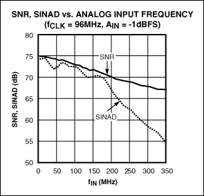
Figure 1. The MAX12559 at 96MHz clock frequency, -1dBFS input, SNR and SINAD and the input frequency corresponding curve.
You can also replace SINAD with effective number of bits (ENOB) to indicate the accuracy of an ADC with a given input frequency and sampling rate. It is actually the ratio of the rms error measured by the analog-to-digital converter to the ideal rms error. ENOB usually depends on the amplitude and frequency of the input sinusoidal signal in the application. This indicator is used to compare the rms noise generated by an ADC with the rms quantization noise of an ideal ADC under the same conditions. For example, the rms noise generated by a 14-bit ADC with an ENOB of 12 bits is the same as The ideal 12-bit ADC (with a full-scale or near-full-scale input signal) produces the same rms noise.
ENOB = (SINAD-1.76) /6.02
Total harmonic distortion (THD) is the root-mean-square sum of all harmonics in the Fourier spectrum of the signal. The first three harmonics concentrate most of the signal energy. For communication systems, THD is usually better than static DC linearity is more important. The device parameters given by most manufacturers include the data of the first 4 or even the 9th harmonic.
MAX12599 is a new dual-channel ADC introduced by Maxim (Figure 2). It integrates two 14-bit ADCs on a single chip. The sampling rate of each ADC can reach 96Msps, and it can collect intermediate frequency and 350MHz baseband signals. This dual-channel ADC has an internal sample / hold amplifier and differential input. For an input of 175MHz, it can obtain a spurious-free dynamic range (SFDR) of 79.8dBc, a typical signal-to-noise ratio (SNR) of 71.9dB, and a SINAD of 70.9dB. (Figure 3), the total harmonic distortion (THD) is -77.9dBc. This ADC works at 3.3V and consumes only 980mW of analog power consumption. 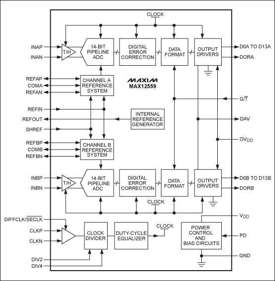
Figure 2. The MAX12559 contains two 14-bit ADCs. Each converter can acquire MAX350MHz IF and baseband signals at a sampling rate of 96Msps. 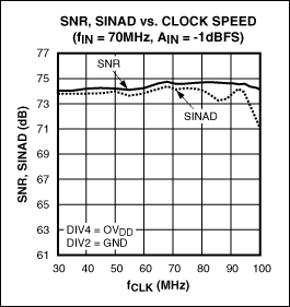
Figure 3. The SNR and SINAD of the MAX12559 ADC are very flat at different clock rates, and the level amplitude measured under the 70MHz input signal is -1dBFS.
The flexible reference architecture allows the device to use a built-in 2.048V bandgap reference or an external reference, and allows two ADCs to share the same reference. The reference circuit can be used to adjust the full-scale input in the range of ± 0.35V to ± 1.15V. The MAX12599 supports single-ended or differential clock input. The user can select the divide-by-2 and divide-by-4 modes, simplifying the selection of the clock source.
The choice of buffers needs to be considered when choosing a buffer amplifier for the MAX12559 or similar high-speed ADC in modern communications receivers. Ideally, the buffer amplifier needs to have the same bandwidth or wider bandwidth as the ADC. The bandwidth of the MAX12559 is 750MHz. It must at least meet the bandwidth requirements of the sampled signal. ADC buffer amplifiers generally define indicators according to frequency domain characteristics, while common operational amplifiers specify settling time and slew rate indicators. No matter how the buffer amplifier defines the specifications, it must have the transient response capability required by the ADC input, so that the input waveform will not be clipped or distorted by more than 1 LSB of the ADC.
At the front end of the receiver, the noise figure of the buffer amplifier also has an effect, but it is not dominant. In the signal link, the first-stage amplifier has the largest impact on the receiver noise figure; usually, the amplifier with the lowest noise figure is placed at the forefront of the signal link. Therefore, a buffer amplifier with a low noise figure helps to improve the noise figure of the entire receiver, but the noise figure of the buffer is not as strict as the first-stage amplifier. If the receiver's first-stage low-noise amplifier has a noise figure of 2dB or less, for a buffer amplifier, a noise figure of 6dB to 7dB will have a minimal impact on the receiver link.
The buffer amplifier should provide sufficient gain to ensure that the signal sent to the ADC is close to the full-scale input voltage. At the same time, the frequency response characteristics should be well controlled. The gain flatness should be kept within one LSB of the ADC. For high-resolution (14-bit or higher) ADCs, the buffer amplifier is required to have a gain flatness of ± 0.5dB over the entire effective bandwidth. The buffer amplifier should provide good linearity according to the output voltage and intercept point. For example, the buffer amplifier must provide at least the output consistent with the input requirements of the ADC. The linearity should be better than the linearity of the ADC to avoid lowering the SFDR of the ADC.
When considering the influence of the phase error of the buffer amplifier and ADC on the spurious characteristics, it can be calculated by the following formula:
SFDR system = -20log {10exp [(-SFDR ADC) / 20] + 10exp [(-SFDR buffer) / 20]} (dBc)
The source impedance of the buffer amplifier should be low enough to ensure isolation from the ADC input impedance and provide enough power for the ADC input drive. In order to avoid additional conversion errors, the high-frequency output impedance of the buffer is also required to be as low as possible. In short, the output impedance of the buffer amplifier will directly affect the AC characteristics of the ADC, especially the total harmonic distortion (THD).
For switched capacitor ADCs, the converter may draw a small amount of input current at the end of each conversion. When using this type of ADC, the buffer amplifier must also have a fast enough transient response capability to avoid conversion errors. If the buffer's transient response is fast enough and the bandwidth is higher than 100MHz (10ns rise time), the error will be minimal. When the transient response of the buffer is not fast enough, an RC filter can be added to its output to limit the input bandwidth according to the requirements of the receiver, and an additional capacitor is provided to eliminate the transient effect of the ADC. The filter capacitor should be larger than the input of the ADC capacitance.
Maxim's MAX2055 and MAX2027 can be used as a buffer amplifier for the MAX12559. The MAX2055 is a numerically controlled variable gain amplifier with a bandwidth of 30MHz to 300MHz (Figure 4). It has single-ended input and differential output, which is convenient for use with differential input ADC. The buffer amplifier integrates a digitally controlled attenuator and high linearity amplifier and a single-ended to differential converter. No external conversion or additional amplifier circuit is required. The MAX2055's built-in attenuator provides an attenuation range of 23dB with an accuracy of ± 0.2dB, which can be used for dynamic gain adjustment or channel gain setting (Figure 5). When set at maximum gain, it has a noise figure of 6dB (Figure 6), and has an output third-order intercept point (OIP3) of + 40dBm at all gain settings (Figure 7). The maximum output power at the 1dB compression point is + 24dBm, with a second harmonic (HD2) of -76dBc and a third harmonic (HD3) of -69dBc.
The MAX2027 also has DVGA functionality, but it is a single-ended device with an adjustable gain range: -8dB to + 15dB, an adjustable step difference of 1dB, and a signal bandwidth of 50MHz to 400MHz. The noise figure is 4.7dB at the maximum gain setting, and has an OIP3 of + 35dBm at any gain setting point, and the attenuation accuracy is maintained at ± 0.05dB. 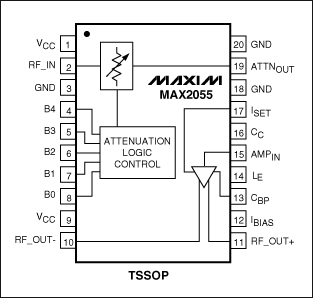
Figure 4. The MAX2055 buffer amplifier includes a digitally controlled attenuator and a single-ended to differential amplifier to provide a flexible interface for high-speed ADCs. 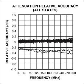
Figure 5. The precise amplitude control of the MAX2055's internal attenuator is very suitable for the gain stage circuit of a differential ADC. 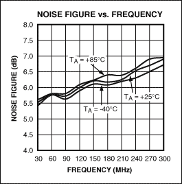
Figure 6. The MAX2055 buffer amplifier has the lowest noise at its maximum gain. 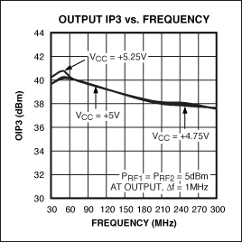
Figure 7. The MAX2055 can increase OIP3 by + 40dBm for all gain settings.
Optimize buffer amplifier / ADC connection
Abstract: With the improvement of the digitization of receivers, the conversion of analog signals into the digital domain has become the key to improving the dynamic performance of communication equipment. This article discusses in detail the key parameters that need to be considered when selecting appropriate signal conditioning and conversion devices for communications equipment.