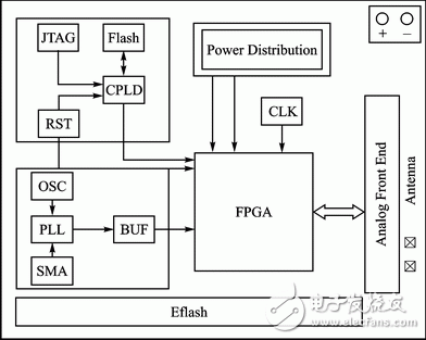
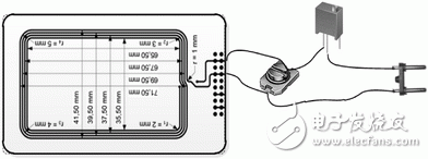
Abstract: With the development of integrated circuit design technology and the improvement of chip integration, verification has become the main bottleneck in the chip design process. This paper designs an FPGA-based smart card verification platform and elaborates on the verification method. The successful practice of dual-interface smart card chip verification is not only a confirmation of FPGA verification theory, but also the verification ideas and methods have certain guiding significance for other chips. Introduction With the continuous development of EDA technology and semiconductor manufacturing processes, single-chip functions are becoming more and more powerful, structures are becoming more and more complex, and design and manufacturing costs are also greatly increased. Especially after entering 90 nm, the overall design cost of the chip has increased by about 20%. Even with the 130 nm process, the cost of a single chip manufacturing is hundreds of thousands of dollars, which makes the verification work play a role in the whole design process. The more important. Verification through the entire process of integrated circuit design, from the development of the system SPEC, verification work has begun, from architectural design, behavioral level system modeling to modular design and implementation, to the generation of netlist and back-end layout, wiring, etc. In the series process, the verification work has been accompanied by it. Through the verification of each stage, the problem of the previous stage can be avoided to take the next stage. Today, the entire integrated circuit industry has gradually formed three major industries: IC design, chip manufacturing, and chip packaging. In the IC design industry, the development of design and verification is uneven, and the development level of verification technology lags far behind the development level of design. For verification, the traditional method is to achieve the purpose of verification design through software simulation. However, due to the limitations of software simulation speed and simulation model, when the complexity and scale of the chip reach a certain level, verification is often difficult to achieve satisfactory results. Especially for the simulation front-end verification, due to the limitations of the simulation model, the simulation results are inconsistent with the actual device operation, and it is often difficult to ensure the reliability of the designed circuit. In order to overcome the shortcomings of the existing verification methods in terms of efficiency and reliability, this paper provides a new verification platform. On the one hand, the verification platform can implement the hardware module in the design of the smart card chip, so that the software can run at a high speed in a real hardware environment, thereby verifying the feasibility of the design functionally; on the other hand, the verification platform can directly interact with the MP300 TCL2. The non-contact smart card tester and various card readers communicate, and in different communication environments, by adjusting the performance parameters of the verification platform itself, the optimal working mode can be found, thereby providing a reference for improving the performance of the design. . The overall design scheme of the smart card verification platform based on FPGA is shown in Figure 1. The verification platform is mainly composed of an adjustable coil, an analog front end component, a digital logic component and a memory component. The adjustable coil is a channel for the analog front end to obtain energy and signals. The analog front end modulates and demodulates the signal, and provides energy for the digital part and the memory. The digital logic part performs signal processing, and the memory performs system software and user data. store. The verification platform realizes the basic functions of the contactless smart card, and can directly communicate with the commercially available card reader, and can verify the rationality of the design scheme by verifying the analog or digital signal on the platform during the test communication process. Figure 1 Overall design of the smart card verification platform 1.1 Adjustable coil design The induction coil part of the adjustable coil is made of non-contact smart card base, the inductance value is 2.1 μH; then an SG1036ND adjustable capacitor is connected in parallel with the induction coil, and its capacitance value is from 0.9~ 30 pF adjustable, calculated by the resonant frequency formula: ω = 1 / L & TImes; C knows that in the case of constant inductance, the resonant frequency of the resonant circuit can be changed by changing the capacitance value in the resonant circuit; Connect a 3296W-101 type adjustable resistor in series, the resistance value is adjustable from 0 to 100 Ω, and the formula of quality factor (Q value) is calculated: Q=(1/G)C/L, by changing the resistance in the resonant circuit The Q value of the resonant circuit can be changed accordingly. The structure of the adjustable coil is shown in Figure 2. Figure 2 Structure of the adjustable coil From the above, the adjustable coil of the verification platform can realize the flexible adjustment of the resonant frequency and Q value of the contactless smart card. 1.2 Analog Front End Component Design The analog front end component consists of LDO chip AMS11173.3 and AMS11171.8, antenna interface, interface with digital logic and analog front end chip BES2416C. The main function of the analog front-end components is to verify the analog part of the smart card chip. In order to ensure that each part of the circuit can be effectively verified, most of the internal circuit components of the BES2416C are consistent with the smart card chip, including rectifier circuit, current limiting circuit, and clock extraction. Circuit, phase locked loop, reference voltage generating circuit, power-on reset circuit, modulation circuit and demodulation circuit. The difference between the analog front-end chip and the smart card is that the smart card can only be sealed by the contact Vcc, RST, CLK, GND, and DATA signals. The analog front-end chip BES2416C is a 64-pin package that simulates digital interaction. The signal and the signal characterizing the working state of each part of the analog circuit are pulled out to the outside of the chip through the pin, so that the working state of each part of the analog front end can be monitored in real time by measuring the above signal, and the designer can help the designer to find out Design the best working mode of the circuit and design this mode into the smart card chip. 1.3 Digital Logic Component Design The digital logic component consists of Xilinx's XC5VLX110 FPGA chip, an interface that interacts with the analog front end, and an interface that interacts with the memory. The main function of digital logic components is to verify the digital part of the smart card chip. This paper uses FPGA-based fast system prototype verification. The essence of this verification method is to quickly implement the hardware module of the digital logic part in the smart card chip design, let the software The module runs at high speed in a real hardware environment, enabling hardware and software co-verification of the design. Since the smart card chip adopts low-power design and uses more gated clocks, this paper chooses an FPGA chip with more global clock networks, which contains 110 000 logic units, 32 global clock networks, and 1 200 user I/O, 16.4 Mb block storage area. Since the biggest feature of FPGA is static programming or online dynamic reconstruction, the hardware function can be modified by programming like software. Therefore, this verification platform can not only verify the digital logic that has been designed, but also the design process. The modified part of the digital logic is verified in real time. 1.4 Memory Component Design The memory component consists of an LDO chip AMS11173.3 and AMS11171.8, a 64 Kb Eflash chip BES2416B_E, and an interface that interacts with digital logic. The main function of the memory component is to verify the Eflash part of the smart card chip. The IP core inside the Eflash chip used in this paper is consistent with the smart card chip, and is 64-pin package. All address bus, data bus and control signals are pulled through the pins. Out of the chip, you can use the digital logic in the FPGA to control its read, erase, and write operations. Therefore, the chip can not only store the on-chip operating system and data as a memory, but also visually verify whether the digital logic in the smart card controls the timing of the Eflash. correct. The verification method is divided into two parts: functional verification and performance verification. The verification method of this platform is described in detail below. 2.1 Functional Verification The digital logic of the first two steps of the communication between the verification platform and the reader is implemented in the FPGA. If the reader first sends a card seek request signal, the verification platform can respond, and the reader is in the second step. The card can be successfully selected, indicating that the receiving and transmitting functions of the verification platform are normal. Otherwise, the signals on the test points of each component can be tested according to the working sequence of each module in the communication process to locate the problematic module. Further verifying the erasing function of the Eflash, the card reader sends instructions for reading, erasing, and writing Eflash to the verification platform respectively. If the verification platform returns a signal indicating successful operation to the card reader, the Eflash function is normal, and the memory component test is required to be tested. The signal on the point finds out the problem with the timing in the Eflash operation, and then modifies the code to reimplement the digital logic in the FPGA. In summary, if the above three steps are verified, it can be stated that the designed smart card chip is functionally normal. 2.2 Performance verification Resonance frequency and Q value adjustment: ISO/IEC 14443 protocol specifies that the non-contact smart cartoon credit carrier frequency is 13.56 MHz ± 7 KHz, but the resonance frequency of the smart card itself does not specify the standard value, therefore, objective This has resulted in a diversity of resonant frequencies of smart cards currently in circulation. Through testing, it is found that the performance of smart cards at different resonant frequencies is different. Each smart card manufacturer's chip has its own optimal operating frequency range, but this region cannot be located simply by theoretical analysis, and the verification platform can be adjusted. The adjustable capacitance on the adjustable coil changes the resonant frequency of the verification platform, so it can communicate with the reader at different resonant frequencies to find the optimal resonant frequency for the smart card chip to work. Similarly, by adjusting the adjustable coil Adjusting the resistance to change the Q value of the verification platform can find the Q value that is most beneficial to the operation of the smart card chip. Verification of the field strength range: ISO/IEC 14443 Type A protocol stipulates that contactless smart cards should operate normally in the field strength range of 1.5 to 7.5 A/m. The verification platform can communicate normally with the MP300 TCL2 non-contact smart card test instrument. First, the adjustable coil is placed on the test stand of the TCL2 and the magnetic field intensity emitted by the TCL2 is adjusted to 1.5 A/m, and then tested according to the functional verification steps. If the function of the smart card under 1.5 A/m field strength is verified by verification, the field strength is adjusted to 1.6 A/m for the same verification, and the verification platform is operated from 1.5 to 7.5 A/m according to the above method. Statistics, and then test the field strength area of ​​the verification platform communication abnormally, test the signal on each component test point according to the working sequence of each module in the communication process, locate the problematic module and improve the design of the module, then repeat the The verification process works until all field strength points are working, and finally the verified circuit structure is designed into the smart card. Receive performance verification: ISO/IEC 14443 Type A protocol stipulates that the signal sent by the reader is 100% ASK modulation, the data sent by the reader is 0, and the waveform of pause is determined by four parameters t1, t2, t3, t4. And gives the range of values ​​for these four parameters. According to the test experience, the receiving performance of the smart card is determined by t1 and t2, and the smart card receiving is the most difficult when t1 and t2 are the two limits. The two extreme cases are: t1=3 μs, t2=0.5 μs And t1 = 2 μs, t2 = 0.7 μs. First, put the adjustable coil on the test stand of TCL2 and adjust the pause waveform sent by TCL2 to a limit condition, and then follow the steps of function verification. If the verification shows that the smart card receives well under such limit conditions, Then adjust the pause waveform to another limit case for the same verification. If the verification platform cannot communicate normally under any one of the conditions, configure the control word of the demodulation circuit demodulation threshold adjustment in the analog front-end chip, and then perform the reception performance again. The verification is repeated until the verification platform works normally under the two extreme pause waveforms, and finally the working mode of the verified demodulation circuit is designed into the smart card. Verification of transmission performance: ISO/IEC 14443 Type A protocol stipulates that the load wave modulation depth transmitted by the smart card should be at least 22/H0.5 mV. First, place the adjustable coil on the test stand of TCL2 and adjust the magnetic field intensity emitted by TCL2 to 1.5 A/m. Then use the ISO 103736 test script of TCL2 to calculate the load modulation depth at the current field strength and perform the required value with the protocol. Comparison, if the requirements are met, the load modulation depth of the smart card is good at the current field strength, and the field strength is adjusted to 2.0 A/m for the same verification. The verification platform is loaded from 1.5 to 7.5 A/m according to the above method. The modulation depth is calculated. If the load modulation depth does not meet the protocol requirements under certain field strengths, the control word of the modulation circuit load modulation depth in the analog front end chip is configured, and then the transmission performance is verified again, so as to repeat the verification platform. The load modulation depth satisfies the protocol requirements at each field strength point, and finally the working mode of the verified modulation circuit is designed into the smart card. Verification of Eflash operation time: TBIT is a signal indicating the operating state of the Eflash chip of the verification platform. When the TBIT signal is high, it indicates that it is operating, and the TBIT signal is low, indicating that the operation is completed. The operation of Eflash includes three actions of reading, erasing and writing. The following three times are verified respectively: firstly, the adjustable coil is placed on the card reader coil and one channel of the oscilloscope is connected to the TBIT signal test. Point, then the card reader sends a command to read the 1 byte in the Eflash to the verification platform, and captures the duration of the high level of the TBIT signal through the oscilloscope. This time is the time when the Eflash reads 1 byte; the card reader Sending a command to erase the 1 page of the Eflash to the verification platform, and capturing the high level of the TBIT signal by the oscilloscope for a duration of time, this time is the time when the Eflash erases 1 page; the card reader sends the write to the verification platform to the Eflash 1 The instruction of the byte, the time taken by the oscilloscope to capture the high level of the TBIT signal, this time is the time when Eflash writes 1 byte. After the above verification of the Eflash operation time, the R&D personnel can accurately calculate the time required for the hardware operation during the interaction between the smart card and the card reader, and use this time to compare the actual smart card operation time to evaluate the efficiency of the on-chip operating system. Provide a reference for the improvement of software performance. In summary, these verification methods can help developers to find out the shortcomings in chip design in time, so as to improve before the tape is released, and improve the success rate of smart card chip development. Conclusion This platform can be applied to the design verification of other communication chips and has good engineering application value. References [1] Huang Li. FPGA Verification of Million Gate Level ASIC [D]. Xi'an: Xi'an University of Electronic Science and Technology, 2007:16. We provide quick-turn injection molding by many types of materials, like ABS, PA66, PBT, TPU, TPE, PVC, PE, NYLON 6, PC, silicone, TPE, EPDM, PUR, etc. Special for some plastic parts. Our advantages in internal prototyping, bridge tooling and short-run manufacturing, which can eliminate the costly and time-consuming for customers a lot.
ETOP experienced to support one-stop cable assembly solution service, including wire harness, palstic enclosure, silicone, metal, PCBA, etc.
Injection Molding Parts,Plastic Injection Molding,Low Cost Plastic Injection Molding,Plastic Mold Injection Molding ETOP WIREHARNESS LIMITED , https://www.etopwireharness.com
The card reader is used to write the on-chip operating system conforming to the PBOC2.0 standard to the Eflash chip, so that the verification platform supports the electronic wallet and the electronic passbook function. If the verification platform can successfully complete the storage, circle, and consumption specified by PBOC2.0. All functions such as balances are taken, indicating that the trading function of the verification platform is normal.
[2] Fu Yongjie. Discussion on the role of FPGA in ASIC design [J]. Electronics Today, 1996 (2).
[3] National Financial Standardization Technical Committee. China Financial Integrated Circuit (IC) Card Specification Part II: Electronic Wallet/Electronic Passbook Application Specification [M]. Beijing: China Financial Press, 2010: 1938.
[4] Zhou Honghua, Li Shuguo, Zhou Runde. Structure and design of high security smart card chip[J]. Journal of Tsinghua University, 2003, 43(4).
[5] Xilinx. Virtex5 FPGA User Guide. , 2009: 2536.
[6] Akihiro Higashi, Kazuhide Tamaki, Takayuki Sasaki. VerificaTIon Methodology for a Complex SystemonaChip [J]. FUJITSU Sci. Tech. J., 2000(6): 2430.
Chen Bo (Master's), the main research direction is chip verification, testing and embedded system design; Yu Zhongchen (Professor), the main research direction is SoC design and embedded systems.