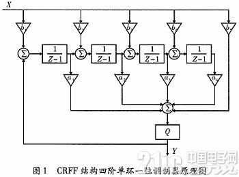
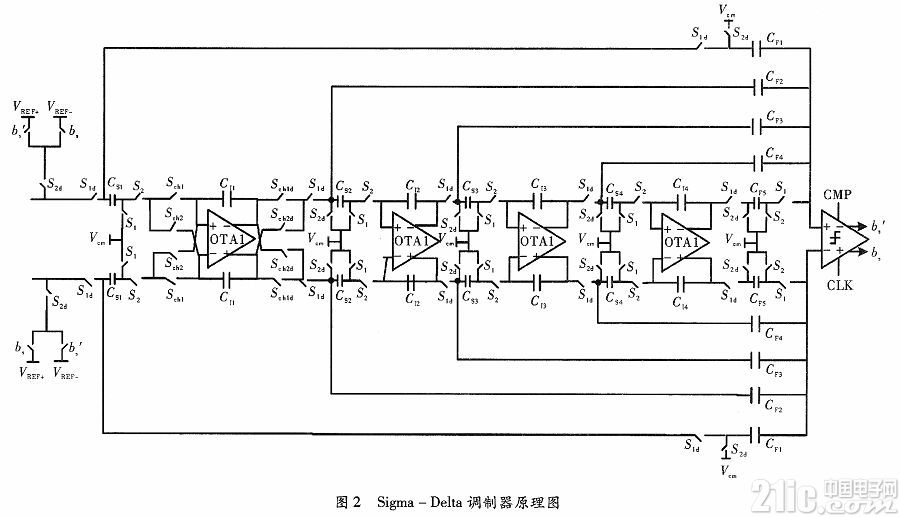
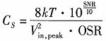
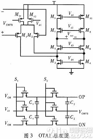
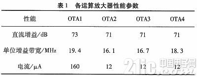
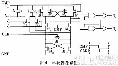
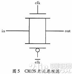
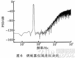
Abstract A high-precision, low-power Sigma-Delta modulator for audio and sensing applications is designed. The modulator uses a four-stage, single-loop, one-bit CRFF structure that reduces the need for even harmonics, substrate and power supply noise, and the use of chopping techniques, reducing DC offset and switching capacitor-type fully differential circuits. Low frequency noise achieves the goal of improving accuracy and reducing power consumption. This design uses the Global foundries 0.18μm CMOS process with a supply voltage of 1.8 V, an oversampling rate of 128, and a sampling clock frequency of 5.12 MHz. The simulation results show that the modulator has a signal-to-noise ratio of 100.2 dB and the entire modulator consumes only 380 μW. This article refers to the address: http:// With the continuous development of semiconductor integrated circuit manufacturing processes, system-on-a-chip (SOC) has become the mainstream of design technology development, and has been widely used in handheld audio equipment and sensors. As we all know, SOC design is based on a large number of reusable intellectual property modules (IP). Among these IPs, analog-to-digital converters (ADCs) have received attention due to the location of bridges connecting analog and digital signals. Due to the limited capacity of the battery in the handheld device and the high requirements for sound quality, the design of the ADC focuses on low power consumption and high conversion accuracy. Among various types of ADCs, Sigma-Delta ADC is the first choice for low-speed, high-precision ADCs, especially in the fields of sensors and speech processing. This paper designs a fourth-order single-loop one-feedforward sigma-delta modulator (the core part of Sigma-DeltaADC) used in the field of audio and sensors. It effectively reduces the use of switched-capacitor fully differential circuits. Subharmonics, substrate and power supply noise; through the use of chopper technology, DC offset and low frequency noise (mainly 1/f noise) are reduced, and the signal-to-noise ratio is improved. The modulator is implemented in a Global Foundries 0.18μm CMOS process with a supply voltage of 1.8 V, an oversampling rate of 128, and a clock frequency of 5.12 MHz. The simulation results show that the modulator has a signal-to-noise ratio of 100.2 dB and the entire modulator consumes 380 μW, meeting the requirements of low power consumption and high precision. 1 Sigma-Delta Modulator System Design 1.1 System structure and parameter design The Sigma-Delta modulator has three important system parameters, which are the quantizer bit number M, the system order L, and the oversampling rate OSR. Different combinations of these parameters constitute a slightly different quantization noise shaping effect. The total energy of the residual noise in the band is inversely proportional to the 2L+1 power of the OSR. Thus increasing the OSR, or increasing L, can significantly reduce residual noise. Increasing the quantizer bit number M will reduce the quantization step. However, if the number of bits of the quantizer exceeds 1 bit, there is a mismatch between the feedback devices, which will reduce the system conversion accuracy. To use the Dynamic Device Randomization Algorithm (DER) to eliminate mismatch, this will increase the design difficulty, so the design uses a 1-bit quantizer. The Sigma-Delta modulator transfer function mainly includes a feedback structure (CRFB) and a feedforward structure (CRFF). Both of these configurations can achieve only the processing of the noise component in the output signal of the integrator, but the implementation conditions are different. In CRFF, the condition to be satisfied is bi = 0 (2 ≤ i ≤ L), and the condition to be satisfied in CRFB is ai = bi (i ≤ L). In contrast, the CRFF structure requires fewer signal branches, requiring fewer switches and circuitry, reducing the noise on the branch and the amplitude of the integrator output signal, thereby reducing the power consumption of the entire Sigma-Delta modulator. . Therefore, from the perspective of low power consumption, this design uses a CRFF structure, as shown in Figure 1. In summary, in order to achieve the design goal, that is, the conversion accuracy is above 98 dB, and leave a certain margin, the final solution that can achieve the design goal is: OSR=128 (OSR is usually 2 N powers) , L = 4, M = 1, CRFF structure. The out-of-band gain of the system transfer function NTF is 1.45 (empirical value|Hinf|<1.5), and the NTF transfer function is integrated by Matlab DStoolbox to obtain the whole system coefficient. 1.2 System circuit design According to the Matlab model, combined with the system working sequence, the block diagram of the audio Sigma-Delta modulator circuit system is shown in Figure 2. According to the system block diagram of the audio Sigma-Delta modulator, a total of 10 clock control signals are required: S1, S2, S1d, S2d, Sch1, Sch2, Sch1d, Sch2d, CLK, CMP. The first four clocks ensure that the system sample integration works properly; the middle four clocks complete the chopper function, and the last two clocks are the comparator clocks. The clocks S1, S2 are non-overlapping two-phase clocks. S1d and S2d are respectively S1, and the upper hop of S2 becomes the same, and the lower hop delays the clock, and the latter groups of clocks are similar. In the system, four OTAs form four cascaded integrators. The gain of the integrator is determined by the ratio of the integrated capacitor to the sampling capacitor. The output of each integrator has a feedforward loop to the quantizer. The reference signal VREF+, VREF- is fed back to the input of the first OTA. The quantizer compares the relative magnitude of the amplitude of the input signal at the end of the S1 phase, enabling digital conversion of the analog input signal. At the S2 phase, depending on the current output digital signal, VREF+ or VREF- is fed back to the input of the first stage OTA to form a negative feedback. The first level of OTA's four chopper switches are used to implement the chopping technique, which modulates the low frequency noise and dc offset to the high frequency band and is finally filtered out by the sigma-delta ADC filter, thereby improving the Sigma-Delta modulator. The signal-to-noise ratio also enables it to be used in the field of ultra-low frequency sensing. 2 Sigma-Delta Modulator Circuit Module Design 2.1 first stage sampling capacitor The value of the sampling capacitor depends on the system design goals. Excessive sampling capacitors will add difficulty to specific circuit designs such as op amps. Conversely, due to capacitive thermal noise, too small a sampling capacitor will increase the thermal noise density of the capacitor. In a two-phase differential system, the derived sampled capacitance value expression can be written as Among them, Vin, peak is the input full-scale signal amplitude, so the minimum value of the sampling capacitor is Cs=1.63 pF. 2.2 Other capacitors Other levels of thermal noise are shaped by the system, and the residual noise in the band is very small. The sampling capacitor can be below 1 pF. For the sake of simplicity, the integral capacitances of the second, third and fourth levels are all set to 1 pF, and then the size of the sampling capacitors at each level can be determined according to the integral coefficient. The feedforward branch thermal noise is also shaped by the system, and the capacitance is also below 1 pF. 2.3 Operational Amplifier In this paper, a fully differential folded cascode OTA with a large output voltage swing is selected for design. In the fourth-order modulator designed in this paper, the gain of the OTA should generally be higher than 60 dB, which can basically meet the requirements for the operational amplifier with folded cascode structure. The gain bandwidth product GBW of OTA usually takes 3 to 5 times of the clock frequency. To save power, the gain bandwidth product should be as small as possible, but too small will reduce the integration accuracy of the integrator and generate harmonic distortion. Therefore, a compromise is made in the power consumption and gain bandwidth product. Common mode feedback circuits are generally classified into switched capacitor type (SC) and continuous time type (CT). Switched-capacitor common-mode feedback saves power and does not limit the output swing of the main op amp. 2.4 Comparator A one-bit quantizer is usually composed of a comparator. Comparators are generally classified into static latch comparators, class B latch comparators, and dynamic latch comparators. Compared with the static latch comparator and the class B latch comparator, the dynamic latch comparator has lower power consumption due to its dynamic characteristics, which is beneficial to reduce the overall power consumption of the chip. Therefore, this paper uses a dynamic latch comparator, the structure of which is shown in Figure 4, mainly composed of pre-amplified op amps and latches. The comparator is controlled by two inverted non-overlapping clocks, where CLK is the comparator operating clock and CMP is the comparison clock, as shown in Figure 4. 2.5 switch In the switched capacitor circuit, due to the non-ideal factor of the switch, there is an on-resistance that affects the performance of the circuit. In order to improve the linearity of the circuit, a CMOS switch of a transmission gate structure is generally used, and its structure is as shown in FIG. This structured switch provides rail-to-rail inverting output with better linearity than a single MOS tube switch. Therefore, the switches in the modulators of this paper all use CMOS switches. In the design, by setting reasonable parameters, the on-resistance of the NMOS transistor and the PMOS transistor are equal, so that the minimum CMOS switch on-resistance can be obtained in parallel. 3 Results and analysis This design circuit is based on the Global foundries 0.18μm CMOS process with a supply voltage of 1.8 V, an oversampling rate of 128, and a clock frequency of 5.12 MHz. The frequency domain characteristic curve of the Sigma-Delta modulator is shown in Fig. 6. The simulation results show that after the chopper technology is used, the input signal and the switched square wave signal are coupled and then synchronously demodulated, the spectrum of the signal is unchanged, and the low frequency noise and dc offset are modulated to the high frequency band, and finally Sigma- The delta ADC filter is filtered out, which effectively reduces the dc offset and low frequency noise. On the one hand, it ensures the accuracy of the modulator, on the other hand, the design can be applied to the low frequency sensor field; through the use of the switched capacitor type fully differential circuit, It effectively reduces the even harmonics, substrate and power supply noise, thus ensuring the accuracy of the entire modulator; reducing the signal branch by using the CRFF structure, thereby reducing the number of switches and circuits, reducing the noise on the branch and The amplitude of the integrator output signal, which significantly reduces the power consumption of the entire Sigma-Delta modulator. The entire modulator consumes only 380μW and has a signal-to-noise ratio of 100.2 dB, achieving high precision and low power. . 4 Conclusion This paper designs a fourth-order single-loop one-feedforward sigma-delta modulator for audio and sensor applications. The modulator is implemented in a Global foundries 0.18μm CMOS process with a supply voltage of 1.8 V, an oversampling rate of 128, and a clock frequency of 5.12 MHz. The simulation results show that the modulator has a signal-to-noise ratio of 100.2 dB and the entire modulator consumes only 380 μW. Through the use of chopper technology, DC offset and low frequency noise are reduced, and the signal-to-noise ratio is improved. Through the use of switched-capacitor type fully differential circuits, even harmonics, substrate and power supply noise are effectively reduced, achieving the goal of improving accuracy and reducing power consumption, meeting high performance and low power consumption requirements. Guangdong Decosun Lighting Technology Co.,Ltd , https://www.decosun-lighting.com