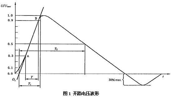
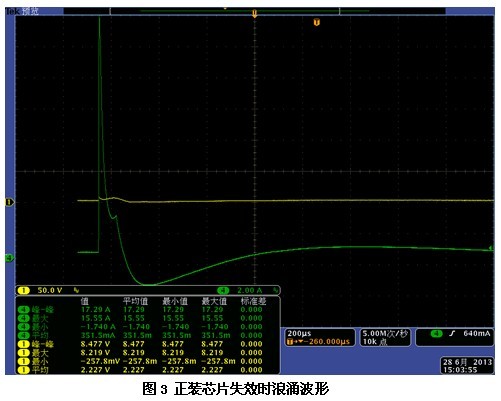
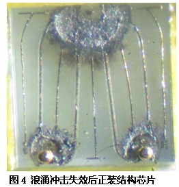
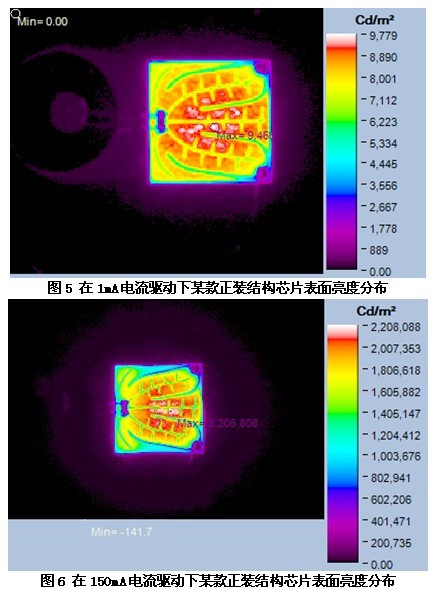
1 Introduction As a new type of lighting technology, LED has the advantages of low energy consumption, long life, small size, dimmable, flexible control and environmental protection. Its application prospects are remarkable. As the price of LEDs declines, the market gradually opens up, and more and more lighting products use LEDs as light sources. Especially in the field of road lighting, high-power LED products have become the protagonist of the market, and LEDs shine in the field of outdoor lighting [2]. However, as the number of LED luminaire applications increases, the number of outdoor LED luminaires that are affected by lightning surges is also increasing. According to the survey, most of the outdoor LED lamps damaged during the normal service life are due to the over-current stress generated by the lightning surge and the lamp power supply and LED light source. This not only affects the service life of the luminaire, but also increases the maintenance cost of the enterprise. In view of this, the lightning surge resistance of LED outdoor lamps should be given enough attention. The lightning surge resistance of LED lamps mainly depends on two aspects: (1) The lightning surge resistance and protection mechanism of LED driving power supply. (2) The ability of the LED chip to resist electrical stress. For the LED drive power supply, it should judge its anti-lightning surge capability by two points: (1) The lightning surge resistance of its own components ensures that the power supply will still work normally after the lightning surge. (2) The attenuation capability of the power supply to the surge current voltage waveform ensures that the peak current and voltage of the attenuation after the surge passes through the power supply are within the range that the LED chip can withstand. Zhang Jinjian [3] of Tianjin University studied the lightning surge of LED driving power supply. According to the characteristics of lightning surge, a suitable power source for LED was designed by using surge devices such as gas discharge tube, varistor and transient suppression diode. The surge protection circuit and the lightning surge generator are used for the immunity test to test its lightning resistance performance. The experimental results show that it can withstand the high voltage of the differential mode 1kV and the common mode 2kV to ensure the normal operation of the LED power supply. However, the lightning surge resistance requirements of LED driver power supplies are determined by the ability of the LED chip to resist electrical stress. Therefore, research on the ability of the LED chip to resist electrical stress is very necessary. Based on this, this paper conducts lightning surge experiments on several types of high-power LED chips to explore the ability of different high-power LED chips to resist electrical stress, to select the driving power and LED chips for LED outdoor lamps, and to resist lightning strikes. The design and development of surge surge capability provides reference and has important practical significance. 2. Influencing factors of LED chip resistance to electrical stress First, the current density that the LED chip can withstand determines its ability to withstand electrical stress. The greater the current per unit cross-sectional area that the LED chip can withstand, the stronger its resistance to over-stress. For conventional electrical conductors, the current density must be low enough to prevent the conductor from melting or fusing, or the insulating material is broken down [4]. Electromigration occurs inside the LED chip at high current densities. When a conductive metal material passes a higher current density, metal atoms migrate and diffuse along the direction of electron motion. Electromigration in the LED freely diffuses metal atoms from one crystal lattice to another. Taking a flip-chip chip as an example, when electron current flows from the interconnecting leads into the eutectic alloy bumps, a sudden change in the geometry of the interconnect leads to the bumps causes current density aggregation and local Joule heating effects at the interface. [5]. The current density aggregation makes the current density distribution in the bump and the chip and the substrate lead uneven, resulting in a complex electromigration force locally generated at the current density concentration, which accelerates the electromigration process and accelerates the LED failure. Second, the current aggregation effect affects the chip's ability to withstand electrical stress. Current concentration is an uneven distribution of current density across the chip, especially near the chip contact point and above the PN junction. The current aggregation phenomenon of the LED chip forms a local hot spot on the chip to form a hot spot, which aggravates the electromigration effect and makes the current density local distribution uneven. The uneven current density causes the local temperature of the chip to rise, and the temperature rise causes the resistivity to decrease, resulting in local The Auger recombination of carriers increases [6], affecting the internal quantum efficiency of the chip. Leakage occurs when minority carriers pass through the charge region of the heterojunction, which causes the injection efficiency of the current to decrease, resulting in uneven illumination and overheating of the LED chip, affecting the luminescence performance and service life of the chip, and eventually causing the LED chip to be short-circuited or open circuit. This phenomenon is especially serious when the chip size and injection current are large. Finally, the current carrying capacity of the LED chip bond wires is a factor that affects the ability of the LED chip to resist electrical stress. Although LED failure is not common in practical applications due to the melting of the bonding wires, the diameter, length, bonding type, physical material properties, and electrical resistance of the bonding wires all have an influence on the current carrying capacity of the gold wires. When the over-voltage is large, the conductor is blown to open the LED. The above factors jointly affect the ability of the LED chip to resist electrical stress. The electromigration and current aggregation effects of the chip can be improved by different chip technology processes. For example, an optimized interdigital electrode can improve current crowding; a vertical structure chip allows current to flow longitudinally within the chip to improve current crowding. At the same time, the number of electrodes and bumps of the flip chip [5], the position and the processing of the ohmic contact have a significant influence on the current spreading of the chip, and the current crowding can be greatly reduced by optimizing the geometry and electrical parameters of the electrode and the Bump. The effect is to improve the non-uniformity of the current density distribution, promote current spreading, and reduce the total equivalent resistance of the chip. It can be seen that LED chips with different structures and different processes have different performances against over-electric stress under the same surge pulse. The following is an experimental study to find the range of single-pulse current peaks of common high-power LED chips on the market. 3. Experiments on different single-pulse currents of different high-power LED chips In order to simulate the impact of actual lightning strikes on LED lamps and chips, the Hangzhou remote EMS61000-5A [7] intelligent lightning surge generator was used to simulate the surge waveform generated in the power grid during lightning strikes. The output waveform of EMS61000-5A is: standard integrated wave of voltage integrated wave 1.2/50μs and current integrated wave 8/20μs [8], where voltage integrated wave (shown in Figure 1) wavefront time: T1=1.67T=1.2 Μs ± 0.36 μs, half-peak time: T2 = 50 μs ± 10 μs. The current integrated wave (shown in Figure 2) wavefront time: T1 = 1.25T = 8μs ± 1.6μs, half-peak time: T2 = 20μs ± 4μs. When the LED whole lamp (including the lamp bead and the driving power supply) is used as the surge test object, it is found that the output surge current of the standard surge waveform after the LED power supply is uncertain, because the lightning resistance design of the driving power supply of different manufacturers is different. The shape of the surge waveform at the output end of the lamp, that is, the input waveform of the lamp bead and the peak current are uncontrollable, which increases the uncertainty during the experiment. In order to solve the above problems, this experiment uses a DC supply to directly supply a single LED, and adds a surge waveform to the DC circuit. The peak value of the current pulse at the input end of the lamp is changed by adjusting the peak value of the pulse voltage outputted by the device and the resistance value in series with the single LED. This achieves the determination of the surge waveform and the controllable magnitude of the pulse peak current. In the experiment, the lamp bead is first illuminated at a working current of 350 mA, and the above pulse waveform is applied in a circuit in which a resistor and an LED lamp bead are connected in series. The pulse voltage is gradually increased from 250V, with an increase interval of 50V. Each voltage file is subjected to a surge impact 5 times, each waveform being separated by 10 s. If the lamp is working properly after the test is completed, proceed to the next voltage level and continue testing. At the same time, the oscilloscope is used to observe the peak current waveform at both ends of the lamp bead. When the lamp bead fails to break down, the pulse waveform is recorded to determine the peak current of the pulse when it fails. (To eliminate the influence of the lamp bead protection electrode on the experiment, the lamp bead protection electrode is removed before the experiment. ). 3.1 sapphire substrate horizontal structure chip anti-surge test A surge test was performed on a horizontally structured LED chip of 45 mil * 45 mil size on the market. Starting from the 250V surge, the lamp beads failed at the 300V second surge. The current surge waveform at both ends of the lamp bead failure is shown in Figure 3. A total of 5 horizontal structure LED lamp beads were tested. The peak currents of the pulse currents were 15.55A, 15.88A, 15.00A, 15.62A, and 15.22A. Analysis of the lamp post after the surge found that the lamp bead was completely short-circuited and the chip electrode was completely broken and blown, as shown in Figure 4: Figure 5 and Figure 6 show the surface brightness distribution of the chip at 1 mA and 150 mA for the sapphire substrate. It can be observed from the figure that the uneven current distribution on the surface of the chip at 1 mA leads to uneven brightness of the chip surface, and the current distribution unevenness increases as the current increases (150 mA).