Fiber Cupboard Qg, China Optical Fiber Cable,GYTA(FS) Anti-rodent Optical Fiber Cable Shandong Qingguo Optical Fiber Co., Ltd. , https://www.qgfiber.com
IntroducTIonThe DS80C320 microcontroller was the first member of the new High-Speed ​​Micro Family from Maxim. The family now includes the DS80C310, DS87C5x0, DS80C390, DS80C400, DS5230, DS5250, among others. When the DS80C320 was introduced, an applicaTIon note 57, " DS80C320 Memory Interface Timing "was published to describe the unique speed requirements for the memories that interfaced to it. This application note serves the same purpose for the more recent family introductions.
A common configuration for a High-Speed ​​Micro-based system is shown in Figure 1. In this example, both program (EPROM) and data (SRAM) memory devices are included in the system. Of course, with an EPROM-based part such as the DS87C520, it is likely that no other program storage will be required outside the processor. However, for the purposes of this discussion, it will be assumed that external program storage will be used. If the application dictates the use of both on- board and external program memories, some additional decoding logic (not shown) may be required so that the two memory spaces do not overlap. 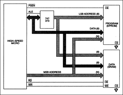
Figure 1. Typical high-speed micro system.
As with all 8051 external memory interfaces, port 0 lines (P0.7–P0.0) of the processor carry both address and data, and a latch is used to demultiplex the information. The specific part number for the latch will be determined by the speed requirements of the system as discussed below. However, in general, the latch will be a '373 or' 573 type. The main difference between these two part types is the pinout. On the '573, all inputs are on one side of the package and all outputs are on the other. This allows a more convenient board layout.
The number of lines connected from the processor's Port 2 address bus (P2.7–P2.0) to the memories' address bus is shown in the figure as' N '. The exact value of' N 'is determined by the storage size of the memory devices used.
This application note is based on the timing of the DS87C520, but the principles discussed herein should be applicable to any member of the high-speed microcontroller family. Be sure to examine the data sheet of the device in use for minor timing differences from the examples here.
Latch RequirementsDue to the high speed of the Port 0 (AD7–AD0) bus, some consideration must be given to the choice of latches used for address demultiplexing. By examining the High-Speed ​​Micro data sheet, it can be seen that some timing constraints are placed on the latch. For instance, the CPU parameter tAVLL (Port 0 Address Valid to ALE Low) determines the minimum setup time (tSU) the latch will actually have. The parameters tLHLL and tLLAX also affect the timing requirements of the latch. Table 1 shows the CPU parameters for 33MHz operation, and the requirements placed on various latch families. For the parameters in the table, the CPU parameters must be greater than the latch parameters. It can be seen that the minimum required setup and hold time are violated for the HC latch family (highlighted). For this reason, this family cannot be used for 33MHz operation.
The other relevant property of the latch is its propagation delay from input to output. Since the latch is in the address path, this parameter has a direct and significant impact on the memory timing requirements. This parameter will be discussed in the following section.
Table 1. Latch Parameters CPU Parameter @ 33MHz Latch Parameter AC Family F Family HC Family tLLHL min 40ns tW 4.5ns 6.0ns 20.0ns tAVLL min 10ns tSU 6.0ns 2.0ns 15.0ns tLLAX min 10ns tH
tPROP 1.0ns
11.5ns 3.0ns
8.0ns 13.0ns
38.0ns
Program MemoryAs shown in Figure 1, the program memory (typically EPROM or flash memory) interfaces to the processor's LSB address through the address demultiplexing latch. The EPROM also interfaces directly with the processor via the MSB address bus and the Program Store ENable (active- low PSEN) signal. The processor always outputs the MSB address before the LSB address, so this interface can be ignored. However, each of the two remaining interfaces must be examined for the most critical timing. The relevant timing parameters for EPROM devices may be found by evaluating their data sheets. Table 2 summarizes the main parameters for several speed grades of EPROMs from two different manufacturers¹.
EPROM Parameters
Note: X / Y indicates difference between the Atmel / AMD devices. Parameter -55 -70 -90 -120 -150 -200 -250 tACC min 55ns 70ns 90ns 120ns 150ns 200ns 250ns tCE min 55ns 70ns 90ns 120ns 150ns 200ns 250ns tOE min 25 / 35ns 30 / 40ns 30 / 40ns 35 / 50ns 65ns 75ns 100ns tDF min 25ns 30 / 25ns 30 / 25ns 35 / 30ns 30ns 30ns 30ns
Upon evaluation of the timing specifications for the processor, the latch and the EPROM, it can be seen that the most critical timing path is through the LSB address bus. The address must appear on this bus, pass through the latch, address the EPROM, and the EPROM must output valid data in less time than the CPU parameter tAVIV1. Since the latch is in the path, the timing of this bus can be expressed by the following equation: tPROP + tACC <tAVIV1. The DS87C520 data sheet shows that tAVIV1 is a function of clock speed (denoted tCLCL), and is given by: tAVIV1 = 3tCLCL-32ns. Solving these equations for 33MHz operation using an F type latch, it can be seen that an EPROM access time of less than 52ns is required. Thish illustrates that the latch speed directly impacts the required speed of the EPROM.
Table 3 shows the EPROM speeds and latch types recommended for various CPU clock speeds. The suggested speed grade is based on the above equation and the EPROM and latch timing parameters. Further evaluation shows that the EPROM parameter tDF may also be a critical parameter at some high CPU clock speeds. This parameter must always be less than the CPU parameter tPXIZ.
Table 3. Recommended EPROM Speeds
* tACC <20ns may require different memory technology. Clock Frequency (MHz) Speed ​​With 'F373 Latch Speed ​​With 'Ac373 Latch Speed ​​With 'Hc373 Latch 33 50 20 * 20 * 25 70 70 50 20 70 70 70 18.432 120 90 90 16 120 120 90 14.746 150 150 120 14.318 150 150 120 12 200 200 150 11.059 200 200 200 7.37 200 200 200 1.8432 200 200 200
Data Memory There are a number of factors that make interfacing data memories (SRAMs) to the High-Speed ​​Microcontroller family extremely easy. First, SRAM devices are generally faster, and more readily available in higher speed grades. In fact, it is sometimes difficult to find a slow SRAM. A more significant factor is that all High-Speed ​​Micro Family members have the ability to insert stretch cycles into the MOVX instructions. This provides a convenient means of supporting both high- and low-speed devices on the same data bus without requiring external support hardware. All High-Speed ​​Micro Family members default to the use of one stretch cycle for MOVX instructions. To obtain maximum throughput, application software can write to certain Special Function Register (SFR) bits and cause the MOVX instructions to operate with zero stretch cycles. This default condition is a convenience to existing designs that may not have fast RAM in place. Even in high-speed systems, it may not be necessa ry or desirable to perform data accesses at full speed. Additionally, there are a variety of memory mapped peripherals such as LCD displays or UARTs that are not fast enough to keep up with the full speed high-speed micro. This flexibility allows the user to trade some performance for slower data RAMs if so desired. For the discussion that follows, a worst case timing scenario of zero stretch cycles will be assumed.
For maximum performance, ie, with a zero stretch cycle data memory access programmed into the processor, a MOVX instruction requires two machine cycles. The fetch of the instruction takes one machine cycle leaving one machine cycle for the memory read or write. In the analysis of the data memory's timing requirements that follows, it will be assumed that the recommendations of Table 3 have been followed.
Through analysis, it can be determined that four SRAM timing parameters are necessary and sufficient to meet the processor's timing requirements for most situations. These parameters and their values ​​for various speed grades are shown in Table 4. During a data read operation, the processor expects the time from an address change until valid data is available to be 71ns (tAVDV1 = 3tCLCL-29) or less. If the propagation delay from D to Q of an F373 latch (8ns) is subtracted from this parameter, you obtain a memory address access (tAA) requirement of 54ns. Also for a data read operation, the time from the active-low RD signal going low until valid data is received from the memory device must be 38ns (tRLDV = 2tCLCL-22) or less. Since the processor's active-low RD signal is tied to the memory's active-low OE pin, the memory must have an output enable access time (tOE) of less than 38ns. After the processor has read the data, the SRAM must relinquish the bus within 25ns (tRHDZ = tCLCL-5). This dictates that the SRAM parameter tOHZ be less than 25ns. For a write, the processor will provide a minimum write pulse of 56ns (tWLWH = 2 tCLCL-5), which is equal to the minimum required write pulse width (tWP) of the SRAM. On the basis of these four calculated parameters and assumed SRAM speeds shown in Table 4, the appropriate speed device may be determined for a number of different clock frequencies. A summary of the recommended RAM speeds is given in Table 5 which assumes the fair F373 latch. It should be noted that the critical timing parameter is not always the access time. Because of the high speed of the processor and variations in memory parameter relationships, all four parameters must be checked for any specific clock speed.
Table 4. SRAM Parameters tAA (ns) tOE (ns) tOHZ (ns) tWP (ns) 35 20 15 25 55 30 25 35 70 35 30 45 80 35 30 60 100 50 35 60 120 60 45 70 150 55 40 90 170 80 35 120 200 100 35 150
Table 5. Recommended RAM Speeds based on tAVDV1 with 'F Latch Clock (MHz) Memory Speed ​​(Zero Stretch) Memory Speed ​​(One Stretch) 33 50 120 25 80ns 200ns 20 80ns 200ns 18.432 120ns 200ns 16 120ns 200ns 14.746 120ns 200ns 14.318 170ns 200ns 12 200ns 200ns 11.059 200ns 200ns 7.37 200ns 200ns 1.8432 200ns 200ns
Additional ConsiderationsAll of the timing calculations used in this application note are based on equations found in the DS87C520 data sheet. These specifications assume an approximately equal capacitive load on the signals specified. If the configuration of Figure 1 is used, this is achieved. If, However, any signal is connected to additional loads, then the capacitive loading including the additional devices should be evaluated. If there is a significant difference, additional margins should be used in the critical path analysis, and appropriate memory speeds selected. For older or otherwise unconventional SRAM devices, it may be wise to confirm other important timing parameters (such as data setup before write active). However, on the devices surveyed, meeting the four parameters discussed above will qualify the device for use.
Equation SummaryFor the user who wishes to calculate the memory speed requirements using a crystal frequency not shown in the preceding tables, the following equations provide a concise summary of the information needed.
EPROM Equations 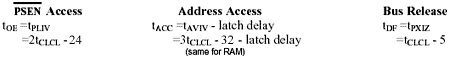
RAM Equations 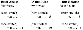
¹EPROM devices from AMD and Amtel were considered.
High-speed Micro Memory Interface Timing-High-Speed ​​Micro M
Abstract: This applicaTIon note addresses external memory interfacing with Maxim high-speed microcontrollers other than the DS80C320. A systems designer using these microcontrollers must be aware of mulTIplexed address / data latch requirements and latch parameters for different families of devices. EPROM and SRAM parameters are discussed to ensure proper matching between the microcontroller and external device.