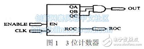
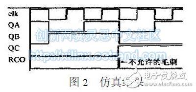
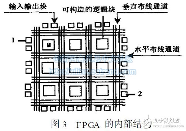
Abstract: Glitches are a common issue in FPGA design, often leading to errors in system performance. This paper explores the root causes and conditions that lead to glitches from the perspective of FPGA architecture. It presents various solutions for eliminating glitches and provides detailed analysis through practical applications. FPGA (Field-Programmable Gate Array) has become a key technology in modern digital communication systems due to its high capacity, flexibility, and reliability. Using FPGAs for digital circuit design is now one of the most popular approaches in the field. However, glitch generation remains a persistent challenge for engineers. These small, unintended signal spikes—known as glitches—are typically caused by internal signal propagation delays within the FPGA. They occur when multiple signals change simultaneously, creating timing conflicts in combinational logic circuits. Since even a single glitch can cause system failure, especially in sensitive circuits like those involving edge-triggered signals, it is crucial to address this issue effectively. This paper analyzes the structural causes of glitches in FPGAs and discusses different strategies to eliminate them, with real-world examples to illustrate their application. To better understand the origin of glitches, let’s look at the example of a 3-bit synchronous counter shown in Figure 1. When the enable signal is high, QA, QB, and QC transition from 000 to 111 on each rising clock edge. After reaching the all-ones state, the carry output should generate a pulse of half a clock cycle. However, according to the simulation results in Figure 2, a sharp spike appears when the counter transitions from 011 to 100, which is a classic example of a glitch. Taking Xilinx's FPGA as an example, its internal structure, as shown in Figure 3, consists of three main components: the Configurable Input/Output Block (IOB), the Configurable Logic Block (CLB), and the Programmable Interconnect Array (PIA). The IOB provides the interface between the internal logic and external pins, while the CLB performs user-defined logic functions. The PIA connects these blocks together, enabling signal routing across the chip. The delay in signal propagation through the PIA and CLB can result in different arrival times for input signals. If two signals arrive at different times, a race condition may occur, leading to a temporary incorrect output known as a glitch. For instance, in the 011 state, if QA and QB switch from 1 to 0 at the same time, but QC changes slightly later, a short-lived high-level pulse might appear, causing a glitch. This phenomenon is directly related to the internal structure of the FPGA and the way signals are routed inside the device. Glitches typically occur under specific conditions. In the case of a 3-bit counter, all three bits—QA, QB, and QC—change simultaneously during a clock cycle. However, due to varying signal path lengths, the arrival times of these signals may not be perfectly synchronized. For example, if QC arrives 2 ns earlier than QA and QB, it creates a brief "all-ones" state, which triggers a false carry pulse. This situation becomes more complex when multiple bits change at once, such as when transitioning from 011 to 100. The mismatch in signal arrival times leads to a race condition, resulting in a glitch at the output. Therefore, the primary condition for a glitch is the simultaneous change of multiple signals, combined with unequal propagation delays. Understanding the conditions that lead to glitches allows designers to implement strategies that reduce or eliminate them. One common approach is to modify the design so that only one bit changes at a time. For example, using a Gray code counter instead of a binary counter ensures that only one bit transitions at a time, thereby preventing glitches. Another method involves adding redundant logic to the design to stabilize the output during transitions. These techniques help improve the reliability and accuracy of digital systems implemented on FPGAs. Redundancy is an effective technique for eliminating glitches. There are two main approaches: the algebraic method and the Karnaugh map method. Both involve adding extra terms to the logic expression or truth table to cover potential race conditions. For example, in a Karnaugh map, if two adjacent cells are connected without overlap, there may be a risk of a glitch. To prevent this, an additional cell can be added to the map, covering the overlapping area and eliminating the race condition. However, this method is not always suitable for counters, where glitches are caused by sequential transitions rather than logical overlaps. Solar Panel,,High Efficiency Mono Solar Panels,Bifacial Jinko Solar Panels PLIER(Suzhou) Photovoltaic Technology Co., Ltd. , https://www.pliersolar.com