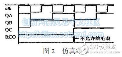
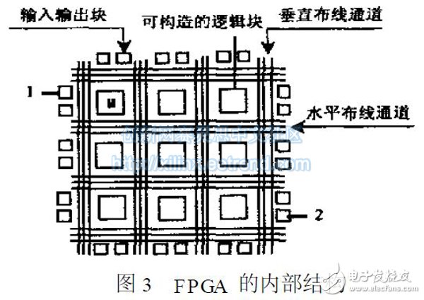
Abstract: Glitches are a common issue in FPGA design and can lead to errors in system performance. This paper explores the root causes and conditions that lead to glitches from the perspective of FPGA architecture, outlines various mitigation strategies, and provides detailed analysis through real-world applications. FPGA (Field-Programmable Gate Array) has become a cornerstone in modern digital communication systems due to its high capacity, flexibility, and reliability. Designing digital circuits using FPGAs is now one of the most widely adopted approaches in digital system development [1]. However, glitch generation remains a persistent challenge for engineers during the design process. These glitches, often caused by signal propagation delays within the FPGA’s internal structure, can significantly impact the efficiency and reliability of the system. Specifically, when multiple signals change simultaneously, small voltage spikes—known as glitches—can appear at the output of combinational logic circuits. These glitches are particularly problematic in circuits sensitive to edge transitions or pulse widths. As such, addressing and eliminating glitches is crucial for ensuring the stability and correctness of digital systems. This paper investigates the underlying causes of glitches from an architectural standpoint and presents a comprehensive review of different elimination techniques. It also evaluates these methods through practical examples to demonstrate their effectiveness in real-world scenarios. To illustrate the cause of glitches, consider Figure 1, which shows a 3-bit synchronous counter. When the enable signal is high, QA, QB, and QC transition from 000 to 111 on each rising edge of the clock. After reaching the all-ones state, the carry output generates a high-level pulse lasting half a clock cycle. However, as shown in the simulation results in Figure 2, a sharp pulse—known as a glitch—appears when the state changes from 011 to 100. Taking Xilinx's FPGA as an example, the internal structure is composed of three key components: the Configurable Input/Output Block (IOB), the Configurable Logic Block (CLB), and the Programmable Interconnect Array (PIA). The IOB provides a programmable interface between the internal logic and external pins. The CLB serves as the core logic unit, capable of implementing user-defined functions. The PIA connects the logic blocks and facilitates signal routing across the chip. As illustrated in Figure 3, differences in signal path lengths can result in varying delays, leading to potential competition between signals arriving at the same logic block. This competition may result in temporary incorrect outputs—glitches. For instance, in the 011 state, if QA and QB transition from 1 to 0 while QC transitions from 0 to 1 with a delay of 2 ns, this creates a brief high-level signal, forming a glitch. Therefore, the fundamental cause of glitches in FPGA design lies in the inherent signal propagation delays within the device. Using the same example, we can analyze the conditions under which glitches occur. QA, QB, and QC all trigger on the rising edge of the clock, but due to differences in signal routing, they may not arrive at the flip-flops simultaneously. If QC arrives 2 ns earlier than QA and QB, it creates a short-lived "all-ones" condition, causing the carry output to generate a sharp pulse. Notably, when transitioning from 011 to 100, two of the three bits change at the same time. Due to signal propagation delays, these changes may not reach the final logic gate at the same time, creating a race condition. The resulting error in the output is what we call a glitch. Thus, the primary condition for a glitch is the simultaneous change of multiple signals. Understanding the conditions that lead to glitches allows designers to modify their circuits and eliminate the risk of such issues. One common approach is to use Gray code counters instead of binary counters, as they ensure only one bit changes at a time, thereby preventing glitches. Another method involves modifying the circuit design to minimize the impact of glitches. Below are some commonly used techniques: There are two main approaches to eliminate glitches using redundancy: algebraic methods and Karnaugh map techniques. Both involve adding redundant terms to the logic function to eliminate hazards. The algebraic method modifies the Boolean expression, while the Karnaugh map method adds extra groups to cover critical transitions. For example, if two adjacent cells in a Karnaugh map are tangent, a hazard may occur. By adding an overlapping group, the hazard can be eliminated. However, this method is less effective for glitches generated in counter circuits, where multiple bits change simultaneously.
All black solar panels or black frame Solar Panel, power range around 400w to 460w which is higher solar panel efficiency the front black or front and back are both black.
All black solar panel data
All Black Solar Panel,Trina Solar Panel Vertex S,Mono Crystalline Pv Modules,Full Black Solar Panels 420Watt PLIER(Suzhou) Photovoltaic Technology Co., Ltd. , https://www.pliersolar.com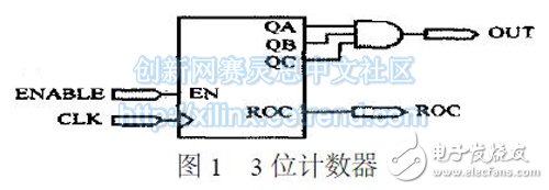
mono type
mono crystalline half cut cell
power range
400watt to 460watt
dimensions
1176*1134*30mm
type
monofacial type or bifacial type
Product details and pic

