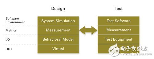
Consumer electronics replacement cycles are getting shorter and shorter, and functional complexity is increasing, making system developers face serious challenges in shortening product development time. Fortunately, today's automated test systems have begun to introduce open FPGAs that will facilitate the integration of the EDA development environment with measurement software, allowing engineers to simultaneously design and test systems and accelerate development time. One of the biggest challenges faced by test engineers today is that personal ideas are limited to the current technology and are stagnant. Therefore, this article provides specific knowledge of technology trends, and it is important for the test and measurement industry to explore the industry. Technology and methods. Design and test and behavior trends For current R&D units, shortening the product development cycle is almost a top priority, especially in the automotive and aerospace industries. One way to reduce development time is to design and test at the same time. Such product development models are often represented by the “V-diagram†model (Figure 1). The final products of these industries often form high-complexity “systems in the systemâ€; while V-diagram is “designed†on the left and “test†on the right, the concept behind it is to preliminarily develop a complete system. Test and test subsystems for greater efficiency. As long as it is an industry that requires a high degree of monitoring environment, it is common to synchronize design/test methods such as V-diagram, and other types of devices or industries have gradually adopted relevant examples. Taking the semiconductor and consumer electronics industries as examples, their “short product life cycle†and “increasing product complexity†characteristics are bottlenecks that shorten product development time. Figure 1 V-diagram product development model According to the 2009 McKinsey questionnaire design for the semiconductor industry, the “product life cycle†of the semiconductor industry is almost one of the points in the automotive industry. Another McKinsey survey also pointed out that the average development time for semiconductor new product design is about 19 months, so the researchers concluded that "R&D Excellence" is the key to speeding up development time. Based on business needs, the product development process must pay more attention to the integrity of research and development, so the electronics industry has become more and more parallel to design and testing. The main way to reinforce this example is to improve the link between electronic design automation (EDA) simulation software and test software. Improve EDA/test software links To understand the role of simulation software in the product design process, you must first understand what the software does in the "design" and "test" phases of product development. During the initial design/simulation, the EDA software can model the physical or electronic behavior of the simulated product (Figure 2). The EDA software is basically a utility that presents the output of the DUT through a mathematical model based on a series of inputs, and then provides the relevant measurement results to the design engineer. Figure 2 The role of software in the product development phase In the inspection/certification phase of developing products, the software usage conditions are only slightly different, mainly to automatically measure the actual flaw type. However, the measurement algorithms required for the inspection/certification phase are the same as those used by the EDA software tools, which is similar to the design/simulation phase. At present, the EDA software is developing a function that is to improve the level of software linking functions between the EDA environment and the test software. To further explain, this link function is to enable the existing EDA software environment to drive measurement software, and the measurement automation environment can automatically link to the EDA design environment. One of the advantages of the design and test software environment is that the software provides a richer measurement algorithm at the beginning of the design process. Engineers can not only learn more about their designs at the beginning of the design process, but they can also integrate the data obtained from the inspection/certification process. The second advantage is that the test engineer can accelerate the development of useful test program code in the design process to shorten the time-to-market of complex products. Measuring product design cycle is significantly shortened through EDA software The way EDA connects to test software to improve the design process is to provide richer measurement capabilities. Basically, EDA tools will predict the behavior of new designs through the Behavioral Model. Unfortunately, the fixed-mode design is tested by measurement criteria and is quite different from the measurement guidelines used to test the final product, making it difficult to integrate the simulated and measured data. The industry is now moving toward a “single tool chain from design to test sharing†that allows engineers to bring measurement operations to the design process as early as possible. Serge Leef, vice president and system-level engineering manager at Mentor Graphics, said that after connecting EDA tools and test software, engineers can design test benches simultaneously during product development and get test reports early in the design process. Because engineers can develop and test results at the same time, rather than having to do the work in order, the design cycle can be significantly reduced. For example, a multi-mode radio frequency (RF) power amplifier (PA) for mobile phones is traditionally designed using RF EDA tools such as AWR Microwave Office. Through the EDA environment, engineers can obtain RF characteristic parameters such as efficiency, gain, and 1dB compression point through simulation operations, but the RF measurement criteria that the final product must meet are designed for mobile phone standards. (established by Global System for Mobile Communications / Enhanced Data Rate Evolution (GSM/EDGE), Wideband Code Division Multiplexing (WCDMA), Long Range Evolution (LTE). Prior to this, because of the difference in measurement complexity, it is often necessary to actually measure the DUT in order to obtain measurement data by measuring the "standard specifications" of LTE error vector magnitude (EVM) and adjacent channel leakage ratio (ACLR). But now that EDA software is connected to automation software, engineers can build an EDA environment on an analog device and use a complete measurement algorithm. Because of this, engineers can identify complex product or system-related issues early in the design process, which is equivalent to shortening design time. Safety Light Curtain,Safety Curtain,Laser Safety Light Curtain,Safety Optic Light Curtain,Security Light Curtain,Press Brake Safety Light Curtains Jining KeLi Photoelectronic Industrial Co.,Ltd , https://www.sdkelien.com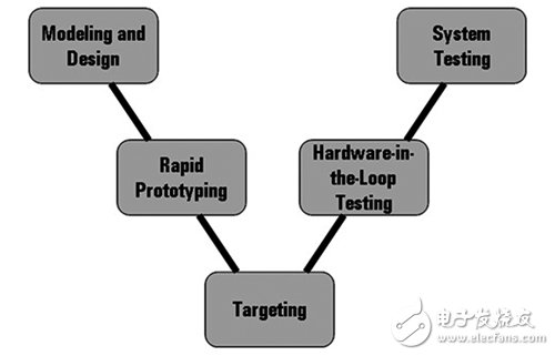
EDA environment connection measurement software electronic product development cycle is greatly shortened
SDKELI has been manufacturing safety light curtains for more than 20 years. Its brand [SHANGSHOU" and [SDKELI" owns largest market share in China because of reliable quality and proper price. All the safety light curtains are type 4 with CE certificate.