Design paperless recorder with C51 and plug-in FLASH Many paperless recorders in the past used 3.5-inch floppy disks as data storage media, but many shortcomings such as poor reliability, limited storage capacity, and high cost of floppy disk storage are difficult to overcome. As a high-tech non-volatile storage device, FLASH flash memory was first used in digital products such as digital cameras, PDAs, mobile phones and other digital products. With the progress of technology and the decline of prices, it has gradually expanded to other application fields. The advantages of large capacity, low power consumption, fast speed, and not easy to be damaged are being favored by people more and more, and the biggest advantage is that with the advancement of technology, the capacity of FLASH flash memory is also increasing, which has been reached 128M, and there is no change in the interface mode, which avoids the time-consuming and laborious redesign. FLASH flash memory is divided into plug-in type and patch type. At present, most domestic manufacturers use the patch type to directly solder FLASH flash memory to the circuit board. This application method makes the FLASH flash memory cannot be changed and moved once it is soldered. The plug-in type can be arbitrarily expanded according to needs and is easy to carry. It is very suitable for applications with uncertain capacity and mobile needs. For these reasons, we have adopted plug-in FLASH as the storage device for paperless recorders. The following is a brief introduction to the design and implementation of a paperless recorder with C51 as the development tool, AT89C55WD microcontroller as the core, and plug-in FLASH as the memory. 1. The overall layout of the paperless recorder The function to be realized by the paperless recorder is this: the recorder has 4 channels, sampling once per second, each channel needs to record two bytes per sampling, according to the dump rate of each channel (from 1 to 255 Can be set), write the sampled data to the external data memory 62256, once the data is full of 512 bytes, write 512 bytes to the FLASH flash memory at once. Figure 1: Overall functional diagram of the recorder The overall function diagram is shown in Figure 1. Second, the system circuit composition The paperless recorder circuit consists of a single-chip microcomputer AT89C55WD, a liquid crystal display circuit, an A / D acquisition circuit, a FLASH flash memory storage circuit, a clock circuit, and a watchdog circuit. The following briefly introduces each component. 1. SCM AT89C55WD and circuit composition The AT89C55WD is compatible with the MCS-51 and can erase and write the core 1000 times. Its voltage, current and power consumption are relatively small, with 20K rewritable flash memory and hardware watchdog timer. The watchdog timer is a method of recovery after the system software crashes. The WDT consists of a 14-bit counter and a watchdog reset special function register (WDTRST SFR). Under default settings, the system is turned off when it is reset. To enable WDT, the user must write 01EH and 0E1H to the WDTRST SFR of the 0A6H unit in sequence. When the WDT is valid, the counter is incremented by 1 after each machine cycle. There is no way to invalidate the WDT except for hardware or WDT overflow reset. When the counter overflows, the WDT generates a reset high pulse on the RST pin. To make WDT continue to be effective, you must write 01EH and 0E1H to WDTRST every certain time to avoid WDT overflow. When the WDT's 14-bit counter counts to 16383 (3FFFH), the counter overflows, causing the device to reset. This means that the user must reset the WDT at least every 16383 machine cycles. To reset the WDT, 01EH and 0E1H must be written to the write-only register WDTRST. When the WDT overflows, a reset high-level pulse is generated on the RST pin, the duration is: 98 × TOSC, TOSC = 1 / FOSC. In order to make full use of WDT, when it is required to prevent WDT overflow reset, WDTRST should be written once every certain period. The single chip AT89C55WD drives the LCD through the P0 port; the sample pulse of the AD7715 is output through T1 and the sample data of the AD7715 is read using the P2.6 pin; because the 8 data lines of FLASH and the address line are multiplexed, the P0 of the single chip is used The port is connected to FLASH through a 74ALS244 and TC4010BP; after using the P2.4 of the single chip through 74ALS32 as the pulse input of the clock DS1305, INT0 is connected to the pin 6 of the clock, that is, INT0, so that the DS1305 generates an interrupt signal every second as AD7715 The beginning of sampling; by using the pulse input to the clock DS1305 as the input of the watchdog X25045, and writing data to the X25045 through P2.6 to realize the watchdog function. 2. Liquid crystal display circuit The HG16501 dot-matrix LCD is used in the recorder, which has a built-in T6963C control chip, which is relatively simple to interface with the single chip microcomputer. 3. A / D acquisition circuit The A / D acquisition circuit is mainly composed of the AD7715. The chip is a serial input, a three-wire interface, and the input of the four channels uses HCF4051. This circuit is mainly a level conversion circuit between 5V and 3.3V, this design uses three TC4010BP to achieve. 5. Clock circuit The system clock adopts the serial clock chip DS1305, and uses Motorola SPI working mode. The INT0 of DS1305 is directly connected to the INT0 of the single chip microcomputer, and the DS1305 generates an interrupt every second to start the AD7715 for sampling. 6. Watchdog circuit The watchdog circuit of the system anti-reset is realized by the programmable X25045. The chip has three functions of watchdog timer, voltage monitoring and EEPROM. This combination reduces the cost of the system and saves board space. 3. System software The system software uses C51 language and A51 assembly language mixed programming, in which the interrupt sampling part is written in A51 assembly language. 1. Programming Language This system uses the C51 compiler of Keil V6.10. A51 is a relocation macro assembler with universal feature machine usage. It is compatible with INTEL ’s MASM51 macro assembly, supports modular programming, and can be easily interfaced with high-level languages, but it is still very different from MASM51. The main reason is that A51 does not support many MASM51 registers. This needs attention. 2. Working process After the system is powered on and the clock, LCD HG16501, and AD7715 chips are initialized, the main program is in the state of detecting the keys of the keyboard cyclically, and corresponding processing is performed according to the keys, and the acquisition part is executed by the CPU generating an interrupt every second. After collecting four channels, first write 512 bytes to the external memory 62256 and then set the write permission. As soon as the main program finds that the write permission is set, it writes the 512 bytes of data to the FLASH flash memory and resets the write permission . Because the software is a hierarchical menu structure, every time you enter the next sub-menu, you must do the same thing, read and display the clock, check whether the write FLASH flash permission bit is set, if set, write data to the FLASH flash, so List it separately as a routine operation. The flow chart of the main program and normal operation is relatively simple, so it is omitted. The flow chart of interrupt collection is shown in Figure 2. 4. C51 and A51 procedures The source program of the C51 part of the entire system software is about 70KB, the A51 source program of the interrupt part is about 7.1KB, the HEX file generated after the two parts are compiled and connected is nearly 16KB, only four fifths of the 20KB program memory is used, and the remaining 4K can be Leave it to add new features in the future. Conclusion In the process of developing the paperless recorder, we used C51 and A51 mixed programming for software development, using FLASH as the memory, not only the software has a lot of functions, but also because the memory is stable and reliable, easy to carry, and also facilitates further data Handle the work. About Silicone Usb Flash Drive Cover:
10.Silicone usb flash drive cover for reference.
Silicone Usb Flash Drive Cover Silicone Usb Flash Drive Cover,Silicone Usb Cover,Silicone Usb Dust Cover,Usb Waterproof Cover,Usb Flash Drive Cover,Micro Usb Cover,Usb Stick Cover OK Silicone Gift Co., Ltd. , https://www.oemsiliconegift.com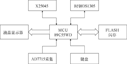

Figure 2: Flow chart of interrupt collection
Silicone Usb Flash Drive Cover is a special protector of usb flash drive.Silicone usb flash drive cover is compact size, shock resistant, damp proof, water proof, lighting resistant, antimagnetic, easy to carry.Besides,it also can as a very especially gift to your family and friend for holiday ,like children on Mother's day, Father's Day, Children's day and Christmas Day ,Valentine's day,The New Year and so on.
Silicone usb flash drive cover introduction:
1.Product name: Silicone USB Cover ,Silicone Usb Dust Cover,Usb Waterproof Cover,usb flash drive cover, Micro Usb Cover , Usb Stick Cover
2.Place of origin:Guangdong China
3.Color:any pantone color
4.Logo:Printing,debossed,embossed
5.MOQ:500pcs.
6.Package:1 pcs/opp,customized design is available.
7.Design:Customized/stock
8.Certification:FDA,LFGB,SGS,ROHS,etc.
9.Usage:Use for usb flash drive cover/Decoration.
