The focus of the hardware design is the PCI bus interface. The PCI bus is divided into 32-bit and 64-bit according to the width of the data bit, and the 64-bit data line is compatible with 32-bit. The 32-bit PCI bus is common in PCs, and its total useful pins are 110, which can be divided into 3 groups. The first group is the basic function signal line, including the 32-bit shared data address line AD [00..31], interface control line, arbitration line, clock line, system reset line, interrupt line; the second group is the additional function signal line , Including error report line, cache function support line, JTAG boundary scan line; the third group is the power line, including the device power consumption marking line, 3.3V power line (12), 5V power line (13), ground line (22 roots). 3 software design The structural block diagram of the software is shown as in Fig. 3. Among them, TM1300 runs pSOS, it is a simple real-time multi-task embedded operating system, with pNA + network components, pNA + is equivalent to the expansion of TCP / IP protocol stack, it provides a socket interface for application programming upwards, and defines downwards An interface for interacting with the network interface layer, including 8 functions, namely: ni_init (initialization of interface chip), ni_broadcast (send broadcast packet), ni_send (send normal packet), ni_getpkb (apply for sending buffer), ni_retpkb (return to receive Buffer), ni_ioctl (I / O control operation), ni_pool (statistic query), Announce (network interface driver calls it to submit the received data packet to pSOS). The network interface layer is the 8029 driver in this application. It drives the 8029 through the hardware abstraction layer. The hardware abstraction layer is a general term for the configuration read and write and I / O read and write instruction sets of the PCI bus. 4 Debugging results Based on the above design, we added a PCI interface on the basis of the original TM1300 video encoding hardware system, and wrote the 8029 driver under pSOS. Then, the data transmission test of the 8029 driver part was carried out on this hardware platform. First, we use a separate UDP sending task to test the sending rate. This task sends a data packet to a PC on the network at high speed, and the size of the data packet becomes longer. The PC receives and counts the number of lost packets. The results are shown in Table 1. Experiments show that there are no errors under the various test rates directly connected by the network cable. After connecting to the LAN, there are a small number of burst errors when the transmission rate is 4.5Mbps. Since UDP is an unreliable transmission method, this kind of error is normal. The maximum rate of UDP transmission in the test can reach about 5Mbps, which is still a certain gap from the maximum rate of hardware (10Mbps). The main reason is that the copy process of data from the system main memory to 8029 on-chip RAM has not yet adopted DMA. It needs improvement. references? 1 Ni Qiang. TM1300-based video surveillance system bit rate control and remote device control interface technology research: [degree thesis]. Nanjing: Nanjing University of Posts and Telecommunications, Department of Information Engineering, 2002 Steel Electric Pole, Electric Power Poles, Terminal Steel Electric Pole YIXING FUTAO METAL STRUCTURAL UNIT CO.,LTD( YIXING HONGSHENGYUAN ELECTRIC POWER FACILITIES CO.,LTD.) , http://www.chinasteelpole.com
Keywords: PCI bus, TM1300, Ethernet communication interface, video communication?
1 Introduction TM1300 is a multimedia DSP launched by Philip. It not only has powerful processing capabilities, but also has very friendly audio and video and I / O interfaces such as SSI and PCI. It can flexibly construct various video communication systems according to the needs of applications. . Before this article, we already have the H.263 hardware and software platform on TM1300, and use the SSI (Universal Serial Port) interface of TM1300 to output the coded code stream. Through two specially designed peripheral interface boards, the modem is used to connect the phone line On the low bit rate transmission and high-speed transmission on the dedicated line through the E1 interface. In view of the current popularity of computer networks and the development of online video services, it is necessary to develop an Ethernet interface for the TM1300 video encoding system to broaden the scope of application. A reasonable way to develop an Ethernet interface is to use the TM1300 integrated PCI interface to drive a dedicated Ethernet interface chip. Because most Ethernet interface chips, such as realtek8029 and realtek8139, are PCI interfaces, you can use the PCI bus to transfer data from TM1300 to these dedicated Ethernet interface chips, and then send data. Moreover, TM1300 can run the embedded operating system pSOS, pSOS with TCP / IP protocol stack, so you can easily complete the TCP / IP encapsulation of the code stream.
According to the above ideas, we first carried out preliminary tests to prove that this is feasible, and then carried out the design of the circuit board, and successfully completed the debugging. At present, this Ethernet interface has been basically developed successfully. This article will introduce the technical points of this design from the hardware and software aspects.
2 hardware design The system block diagram is shown as in Fig. 1. 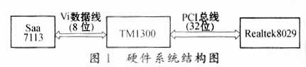
Because the cache function and the JTAG boundary scan function 8029 supported by the PCI additional function signal line are not available, and although the 8029 has a parity error reporting function pin, it can be left unused, so only the first group of function signal lines need to be considered Connection.
The design of the PCI interface has the following main points:
(1) Arbitration of PCI bus.
Two concepts are explained here first. First, the PCI bus is shared by multiple devices. Since there are multiple PCI devices in the PC, an arbiter is required. Second, the PCI device has a master device and a slave device. The master device can initiate the transfer of PCI data. The slave device only It can passively respond to the operation of the master device and respond to read and write operations. The arbitration pins of PCI are REQ # and GNT #, which are called request line and authorization line, respectively. Only the PCI master device has these two pins. REQ # and GNT # are connected to the arbiter in pairs, and REQ # and GNT # of the device are not connected to each other.
The arbitration process of the PCI bus is this: The PCI master device pulls the REQ # level low, indicating that it requests the arbitrator to occupy the bus. After the arbitration is approved, the arbiter pulls the GNT # level of this device low, indicating that the request is approved The device can use the bus. When it no longer uses the bus, make the REQ # signal high, and the arbiter will no longer allocate bus resources to it. In this system, TM1300 is the PCI master device, 8029 is the PCI slave device, and there is no problem of sharing the bus, so there is no need for an arbiter. You can simply short REQ # and GNT #, which is equivalent to TM1300 authorizing yourself.
(2) The PCI_IDSEL signal line plays a key role in the PCI configuration reading and writing of the device.
PCI has a special read and write cycle called configuration read and write. This is when the system boots, and the device has not been configured with I / O or memory addresses. The software can only access the device through configuration read and write. There are two types of configuration read and write, called type 0 and type 1, which one depends on the hardware connection of the bus. When configuring read and write operations without going through the PCI bridge, use type 0, and when going through the PCI bridge, use type 1. The address of type 0 read and write is directly the address on the bus, and the address of type 1 read and write goes through the PCI bridge The decoding becomes the final bus address. In this design, TM1300 and 8029 are directly connected by PCI bus, so type 0 configuration read and write is used.
AD [00..31] is the shared address and data line of the PCI bus. Each PCI transfer is divided into an address cycle and a data cycle. In the address cycle, the contents of AD [00..31] when reading and writing type 0 are as follows: AD [00] and AD [01] are always "00", because the configuration of reading and writing is in double word units; AD [02 〕 -AD 〔07〕 is the register number of the PCI configuration space to be read and written; AD 〔08〕 ~ AD 〔10〕 is the function number of the device. When there are multiple function devices on a PCI card, in order to further distinguish these devices These bits are used, 8029 is a single-function device, these bits are all 0; AD [11]-AD [31] is the device selection bit, there must be and only one bit is "1" (Figure 2 (Shown), this is physically manifested as one of the bus AD [11]-AD [31] is a high level, if the line with a high level is connected to the PCI_IDSEL pin of a PCI card, this piece The card will be activated, and in the following data cycle, it will put the contents of the corresponding registers in its PCI configuration space on the bus for reading. ?
(3) The processing of PCI_FRAME #, PCI_DEVSEL #, PCI_IRDY #, PCI_TRDY # pins.
These four pins are all active at low level, and a pull-up resistor needs to be connected to ensure that the device is in a stable and invalid state when the pin is not driven. The value of the pull-up resistor is in the range of 1kΩ to 10kΩ, the smaller the resistance Then the shorter the time that the chip drives the signal to be effective, but too small will cause the current to be too large, so, to weigh the considerations, this design uses 4.7kΩ.
The above three points have a more general reference significance for the interconnection of PCI devices under offline conditions. In addition, this design has the following special points:
· The PCI_INTA # pin of TM1300 is configured as input to receive 8029 interrupt;
· The PCI clock is provided by TM1300;
· The reset signal of 8029, which is the reset signal of TM1300, is provided by an external circuit;
· The PCI_STOP # and PCI_SERR # pins of TM1300 are floating, because 8029 does not have the corresponding additional function. In addition, the PCI_INTB #, PCI_INTC #, and PCI_INTD # pins of TM1300 can be used as user interrupts. 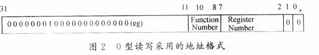

The software execution process is roughly: the system first starts pSOS, pSOS loads the network interface driver, then calls the ni_init function of the driver, initializes the 8029 PCI configuration space and sets 8029 working parameters, and then starts the user task. Here, the user task is the H.263 encoding process. It compresses and encodes the source image read in the VI port, and then calls the socket interface function sendto (sendto is a UDP socket-specific sending function) to send the code stream to pSOS. After pSOS encapsulates according to the UDP protocol, it calls the ni_send function , Ni_send completes the copy of the data packet from the system main memory to the 8029 on-chip RAM, and then starts the 8029 to send data. In the case of reception, after 8029 receives a complete data packet, it notifies the CPU with an interrupt. The CPU switches to the interrupt service routine. The interrupt service routine copies the data packet from the 8029 on-chip RAM to the system's main memory, and then calls Announce The function submits the pointer, data length and other information of the data block to pSOS. PSOS uploads the data packet layer by layer along the protocol stack and makes corresponding processing.
The design of the software is closely related to the pSOS operating system, which is limited in space. This article does not introduce pSOS in detail. You can refer to the relevant contents of references [1] and [2]. In addition, the 8029 driver program can refer to reference [3]. This article focuses on the configuration process of the PCI configuration space. This part has a common reference for similar designs.
The PCI configuration space has 64 bytes. These registers are integrated in the PCI chip, which stores important codes such as the manufacturer's number, device number, and device type of the chip. It also includes command registers, base address registers, etc. that control its bus behavior. Registers, they must be correctly configured when the device is initialized, otherwise the device will not work.
The configuration of 8029PCI space requires three steps:
First, scan the bus. The purpose of this step is to find the configuration address of 8029. Intuitively speaking, which AD line is connected to its PCI_IDSEL pin, because subsequent configuration writes should be addressed based on this address. When scanning the bus, scan each line from AD 〔11〕 to AD 〔31〕. If this AD line is connected to the PCI_IDSEL pin of a PCI device, then use configuration read function to read the PCI configuration space No. 0 When registering, the device and manufacturer code of the device should be returned. If the device is not actually connected to this line, the return value is 0. The device and manufacturer code of 8029 is known as "0x802910ec". If the return value is the same, it means that the device was found. After 8029, it is necessary to write down the serial number of this AD line. For example, if we connect 8029 PCI_IDSEL and AD [20] on the hardware, the scanned serial number should be "20".
Secondly, use the configuration write function to configure I / O read and write enable, that is, write "0x1" in the command register.
Finally, use the configuration write function to configure the I / O address, that is, write the I / O address assigned to the device in the I / O Base Adddress register, such as "0xe400". The program flow chart is shown in Figure 4. 
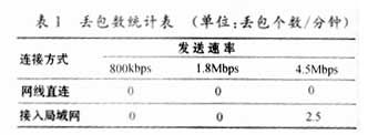
Then, we conducted a joint test of encoding and transmission. The encoding task performs H.263 data compression, and then sends the code stream from the Ethernet interface, and receives this code stream on another PC on the network and performs decoding and playback. The output rate of the code can be controlled by adjusting the quantization step size of the encoder. In the experimental environment, it is found that when the quantization step size is greater than or equal to 5 and the code rate is below 700kbps, there is basically no packet loss, and the decoded image is relatively stable; when the quantization step size is further reduced and the code rate is close to 1Mbps, it In the case of packet loss, colored squares appear in the decoded image. This phenomenon occurs because the H.263 encoder consumes a lot of CPU resources, and the data is copied between the main memory and the 8029 on-chip RAM using I / O read and write methods, which also requires certain CPU resources. When the quantization step size is less than 5, the processing complexity exceeds the capacity of the CPU, thereby generating a certain bit error. The way to solve the problem is to improve the data transmission method (using DMA) on the one hand, and to optimize the coding task on the other hand.
5 Conclusion?
This article focuses on the parts that have a more general reference for similar designs, such as the design of the PCI bus interface and the steps of PCI space initialization. The test results are analyzed in more detail, and the improvement direction is proposed in the future. ?
2 Ni Qiang, Hu Ming. Remote equipment of video surveillance system based on PSTN. Electronic Engineer, 2002 (4): 14 ~ 16
3 Li Peng. Computer communication technology and its programming. Xi'an: Xidian University Press, 1998
Design and Implementation of Ethernet Communication Interface of TM1300 Chip
The design drives the Ethernet chip through the PCI interface of TM1300, and implements an Ethernet communication interface. The program combines TM1300, which is good at multimedia signal processing, and the very popular Ethernet, which can easily realize video communication. The article introduces the design points of the program's software and hardware in detail, and gives the analog data and The experimental results of the actual video compression stream transmission. ?
Yixing Futao Metal Structural Unit Co. Ltd. is com manded of Jiangsu Futao Group.
It is located in the beach of scenic and rich Taihu Yixing with good transport service.
The company is well equipped with advanced manufacturing facilities.
We own a large-sized numerical control hydraulic pressure folding machine with once folding length 16,000mm and the thickness 2-25mm.
We also equipped with a series of numerical control conveyor systems of flattening, cutting, folding and auto-welding, we could manufacture all kinds of steel poles and steel towers.
Our main products: high & medium mast lighting, road lighting, power poles, sight lamps, courtyard lamps, lawn lamps, traffic signal poles, monitor poles, microwave communication poles, etc. Our manufacturing process has been ISO9001 certified and we were honored with the title of the AAA grade certificate of goodwill.
Presently 95% of our products are far exported to Europe, America, Middle East, and Southeast Asia, and have enjoyed great reputation from our customers.
So we know the demand of different countries and different customers.
We are greatly honored to invite you to visit our factory and cheerfully look forward to cooperating with you.