Superior electrical performance Mobile devices such as cellular phones have data or audio interfaces to connect external devices such as microphones, music players, cameras, external storage or multimedia cards. All these I / O interfaces are considered as potential sources and introduction points of conducted and radiated EMI and ESD and other interferences, and these interferences must be completely suppressed. So far, discrete devices have been widely used to implement ESD protection and EMI filtering functions. From the point of view of improving performance and considering the development trend of saving space, this kind of scheme is not suitable for continued use to a large extent. Note The good performance obtained in terms of EMI filtering and ESD protection is due to the use of a dual Zener unit structure designed to achieve these two functions (see Figure 2). This structure is very suitable for designers when there are restrictions on the size of the printed circuit board, especially when using a flip chip package. High integration The effect of the IPAD package Because of the highest functional density per square millimeter, the IPAD circuit is very suitable for high-density circuit boards. In order to maximize the use of IPAD technology, flip chip and QFN packages should be used. Because of reduced parasitic inductance, these packages reduce undesirable high-frequency parasitic components and improve electrical performance. IPAD application examples Figure 4 is an example of the circuit implementation principle (EMIF02-USB01). All the mentioned functions are integrated on a 2.6mm2 silicon chip in a flip chip package. Sheet Metal Cover,Sheet Metal Frame,Sheet Metal Fabrication Frame,Free Sample Sheet Metal Frame Dongguan Formal Precision Metal Parts Co,. Ltd , https://www.formalmetal.com
By integrating various passive and active units on a single silicon chip, IPAD products can integrate various functions required in mobile phone applications, such as ESD protection diodes, EMI low-pass filters, line termination, pull-up or pull-down Resistors, logic switches and RF components. 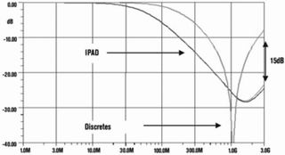
Figure 1 Comparison of attenuation performance between IPAD circuit and passive discrete device 
Figure 2 Equivalent principle diagram of the basic ZRZ unit structure to suppress ESD 
Figure 3 Comparison of SOT and flip chip package filter performance
By integrating EMI low-pass filters, IPAD technology can suppress high-frequency radiation in the high frequency spectrum, which is not conducive to equipment passing EMC standards. Figure 1 compares the attenuation performance of the IPAD filter obtained by the EMIF series with a 33pF discrete capacitor. EMIF devices can attenuate unwanted signals in a wider frequency band.
The attenuation curve of the discrete device scheme using capacitive filtering shows that there is a large attenuation in a very narrow resonance frequency, and a small attenuation at a higher frequency. Discrete device solutions are less efficient for Bluetooth or Wi-Fi exchange protocols.
IPAD devices perform better in the 800MHz to 3GHz range, with attenuation below -25dB. Therefore, the IPAD low-pass filter suppresses the undesired signals of RF devices in GSM, DCS, or Bluetooth devices, and avoids these signals from affecting the baseband chipset and RF module.
In addition to the noise filtering function, IPAD technology also provides ESD protection functions that meet the IEC61000-4-2 level 4 specifications, namely 8kV contact discharge and 15kV air discharge. Due to the integrated double clamp structure, when an ESD surge of 15kV is applied, the output voltage of the device is reduced to 10V.
Obviously, IPAD technology is not limited to the integration of dual zener units, but can also integrate various other components. This allows designers to add more functions to the system by integrating pull-up or pull-down resistors, coupling or decoupling capacitors, Schottky diodes, small-signal transistors, PIN or varactor diodes.
IPAD products integrate passive arrays and networks previously used in discrete devices. Compared with standard discrete devices, the estimated size savings are 50% to 80%. Therefore, this technology is very attractive to designers considering both electrical performance and size.
The dimensions required to implement a 10-stage filter plus ESD protection using IPAD technology and a discrete device solution are as follows. A complete discrete device solution requires a printed circuit board of approximately 19 mm2, while a flip chip package using EMIF10-1K010F1 requires only 6.8 mm2.
For IPAD technology, the performance of flip chip packaging is the best. The intrinsic parasitic inductance of a typical flip chip package is 0.20nH per block, which is much smaller than 0.40nH per lead of the SOT plastic package. The effect of reducing parasitic inductance on the filtering performance is shown in Figure 3. The attenuation gain is about 15% compared with the SOT-323 package.
Figure 3 also shows that the parasitic inductance of the SOT-23 package is 0.55nH per lead. The filter performance is -20dB at 800MHz. For the flip chip package, the filter response at the same frequency is -28dB, and the performance is improved by about 25%.
SIM card interface
The SIM card interface (Subscriber IdenTIfy Module --- Subscriber Identification Module) is a module that is commonly used in mobile phones with removable CPU and memory. This memory card is inserted by the user into the connector on the back of the phone, which exposes the SIM card interface to harmful ESD surges and RF signals transmitted by the antenna.
In order to avoid damage due to ESD or harmful radio frequency signals introduced through the SIM card holder, mobile phone designers usually add an ESD protection and EMI filter circuit between the card holder and the SIM card IC.
In addition to the ESD protection function, the integrated low-pass filter can also suppress RF signals on each data line: RESET (reset), CLOCK (clock), I / O (input / output). This filter is also suitable for GSM, DCS and Bluetooth frequency bands, and uses low-tolerance resistor integration technology to achieve wiring impedance matching.
The connection capacitance can be adjusted according to the GSM 11.1x standard fall time and rise time, not exceeding 50ns.
In addition to the filtering effect, the ESD protection function is divided into two complementary stages (see Figure 2). The ESD surge is clamped by the first stage S1, and then the held voltage is applied to the second stage S2 through the resistor R. This symmetrical structure makes the output voltage very low.
The equation for output voltage clamping is:
Vclamping = Vbr + Rd * Ip
Here Vbr is the diode breakdown voltage, Rd is the dynamic resistance of the diode, and Ip is the peak ESD current.
Assuming that the dynamic resistance of the diode is negligible compared with the filter resistance R and the load resistance Rload, Voutput can be calculated using the following formula:
Voutput = (R. Vbr + Rd. Vinput) / R,
Vinput = (Rg. Vbr + Rd. Vg) / R
Considering the electrical performance of the circuit, when 8kV discharge is applied to the ESD circuit, the calculation result Voutput = 8.4V. Therefore, when an overvoltage occurs, this voltage is kept in a safe range, which fully demonstrates the good performance of IPAD technology.
USB connection in mobile phone
USB is becoming an application method for connecting mobile phones with consumer electronic devices or computers such as notebook computers, PDAs or cameras. USB has the advantages of low speed and high-speed bus up to 12Mbps, which is 100 times faster than the serial port. This data exchange protocol can also automatically detect connected peripherals without shutting down.
On the one hand, this plug-and-play capability makes the system and USB connector susceptible to human influence, and a simple contact may produce harmful ESD discharge. Therefore, the USB connection must comply with the IEC61000 level 4 standard.
On the other hand, especially when we consider wireless applications, the USB connector is a very dangerous point of introduction for the RF signal loop, which may damage the USB hub. This RF effect must be suppressed by the EMI filter in order to comply with the FCC Chapter 15 or CISPR 22 regulations.
The IPAD technology also meets the requirements of the USB 1.1 index regarding USB I / O lines for EMI filtering and wiring. In addition to integrating EMI filtering, wiring loads, and pull-up resistors, IPAD technology also has ESD protection functions that meet the requirements of IEC61000-4-2 level 4, all of which are integrated on a single silicon chip. 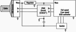
Figure 4 The principle of USB filtering implemented in mobile phones
Compared with SOT-323, flip chip packaging can save 40% of the circuit board space, and has higher filtering characteristics.
The load of the USB connection terminal can be realized by connecting a series resistance to the data line. These resistors match the impedance of the USB cable to ensure proper loading and maintain signal integrity.
The D + and D- lines require pull-up resistors to identify whether the device is full-speed or low-speed. Using IPAD technology, these resistors are integrated on silicon to meet the 5% accuracy requirement in the USB 1.1 specification.
In this example, the low-pass filter consists of a series resistor and a double clamp diode in parallel with the I / O line. In this structure, the frequency attenuation of the RC filter network at 1 GHz is -25 dB.
In addition to the radiated EMI function, the circuit in the above example passed the IEC61000-4-5 level 4 test by placing an ESD bidirectional diode on each I / O data line.
The design of USB applications is critical to meeting the requirements of ESD and EMI filtering standards. The IPAD with flip chip package can make the mobile phone have USB connection, and meet the corresponding standards, provide a fully integrated solution, including impedance matching and pull-up resistors. Moreover, the optimized silicon structure design can meet the 50pF capacitor required by the USB1.1 specification.
IPAD technology is very attractive to designers seeking good electrical performance and saving circuit board size.
Integrated passive and active devices improve mobile phone performance
With the continuous development of mobile phones towards higher integration and more functions, the patented IPAD technology (integrated passive and active devices) has now become a fully mature technology.