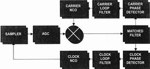
Software Defined Radio (SDR) in the late 1980s, turned to satellite and cellular systems from advanced military and intelligence applications, and will become the mainstream consumer applications, including cellular radio base station, a new generation digital VHF systems, automotive multi-band AM / FM / XM satellite radio, etc. Software radio is a radio whose signal link part is software. It has the following characteristics: Figure 1 shows a general software radio block diagram. Many functions can be implemented in analog or digital form, but the choice must be considered in terms of component availability, complexity, and cost. Typical software transmitter components include: The software receiver components include: The programmability of the radio allows the user's multi-band, multi-mode transceiver to have the following modes: The problem is to design as complete a linear and time-invariant transmitter and receiver hardware as possible, so that the system can provide a "clean" input signal to the digital signal processing hardware, so that a common signal link under software control can be used for all Operating mode. That is, the receiver structure is dependent on ADC selection, determines the available ADC dynamic range. A single ADC can oversample or undersample the modulated signal, perform down conversion in processing and provide I and Q outputs with 4x sampling . However, the higher the sampling frequency, the greater the effect of aperture error. Due to clock jitter, the effective number of bits will be affected. Therefore, there is always an inherent compromise between speed and resolution. The single ADC can realize the functions such as FPGA or receiving signal processor ( dedicated digital chip ) after the digital down-converter with numerically controlled oscillator (NCO) , and can also filter and decimate before the signal reaches the DSP for demodulation.  Picture 1   Software Radio Block Diagram Picture 2  Necessary software to establish recovery time, phase and amplitude In contrast, using an analog demodulator with analog baseband in-phase (I) and quadrature (Q) outputs eases the burden on the ADC and allows additional passive filtering of the baseband to reduce the required dynamic range. The disadvantage is that it leads to quadrature instability, which is due to the phase and amplitude mismatch in the I and Q channels. Two matched anti-aliasing filters ( which can be doubled as channel filters ) and matched ADCs ( or matched S / H amplifiers and a single ADC) are also required . Another design compromise is between analog and digital filtering. Passive analog filter having a low intermodulation distortion and not power, but it has a combined delay, occupies a significant amount of board space (especially at low frequencies) and the trade-off considering the cost, bandwidth, and the Q value. The digital filter may be designed to have a performance close to the ideal, but also have to consider the speed - power tradeoff, tap or more higher operating frequencies require more DSP MIPS, FPGA dedicated hardware or a reception signal processor (available Provide down conversion, decimation and filtering ) . The dynamic range of the ADC is a basic compromise between analog and digital filtering: analog filtering reduces the dynamic range required by the ADC more , and the passive filter does not consume power, while the digital filter increases the dynamic range required by the ADC , But digital filters can have characteristics close to ideal. For linear systems, the ADC must adapt to all desired signal plus interference plus attenuation tolerance and automatic gain control (AGC) response time. The calculation to determine the ADC dynamic range must include: Generally, wideband receivers have a wider ADC dynamic range and smaller total gain (~ 35dB) and narrower AGC range (~ 10dB) than narrowband receivers . The system design also includes cascading noise figure and monitoring analysis and frequency planning. Frequency planning is a skill. Designers must carefully select the system clock, intermediate frequency, and local oscillator frequency to minimize internal and external interference. Not paying attention to the system clock will be an incomplete frequency plan. The system clock is usually a multiple of the frame rate of the encoded data. It is also often a multiple of the channel spacing, allowing the use of integer N phase-locked loops (PLLs) . A complete design also includes the total system calculations for the minimum and maximum input signal levels. A set of calculations for the minimum input signal is performed with AGC turned off without gain reduction, and a set of calculations for the maximum signal level is performed at AGC The full operation is performed with the maximum gain reduced. This also includes intermodulation distortion (IMD) effects of minimum and maximum signal levels . A sensitive point of system design is the AGC system. In software radio, AGC maintains system linearity by reducing the gain of large signals. Set the AGC threshold in this way : C / N increases linearity until the optimal C / N is reached, and then decreases the gain. The set AGC threshold should also allow the ADC a margin, so that the AGC system has time to respond to rapid changes in the input signal and avoid overload. AGC has two basic implementation methods: feedforward and feedback. AGC implementation A typical feedforward AGC system uses a logarithmic amplifier to measure the input signal ( usually at the intermediate frequency ) and juxtapose the downstream gain to maintain a constant signal level in the AGC . This is the fastest response system, but calibration is required because it relies on the accuracy of the scaling factor (dB / v) of the logarithmic amplifier and variable gain amplifier . A typical feedback AGC system compares the detected signal with the reference and uses feedback to keep the detected signal level constant. The system should have a fast start ( gain reduction ) and slow ( gain increase ) AGC time constant. It requires linear dB gain for a stable loop . The signal path latency allows the receiver to be blocked by strong signals. For example, an analog AGC with a peak detector ( at IF) is used to charge the AGC capacitor for several cycles before the feedback is valid . The detector in the baseband is used to calculate the signal level value from the I and Q baseband values, but the latency is worse than the AGC value expected by the IF , especially when it is calculated in the DSP . When changing the frequency, the setup time of the PLL must also be considered . This time delay will cause a waiting time through the system. For example, the time to change the frequency must include PLL settling time, AGC response time, signal propagation time from antenna to ADC , ADC conversion time, and DSP signal processing time. The related demodulation in DSP is the most complicated structure, and the best structure is shown in Figure 2 . The matched filter is usually a maximum likelihood detector (MLD) or a square / quadrature detector for binary phase shift keying (BPSK) and quadrature phase shift keying (QPSK) , respectively . If additional processing of MLD can be handled , the gain of low signal tracking performance may be 6 dB or higher. In many cases, the carrier and clock are recovered by the PLL . The input is generally oversampled and stored in a circular buffer. The read flag for this buffer is the output of the NCO 's clock loop filter. In addition, an interposer through the ADC or direct sampling can be used . The composite mixer ( at baseband ) distinguishes between positive and negative frequencies. They also do not require low-pass filtering to remove mixing components. The output of the mixer is fed into a matched filter unit, which uses a maximum likelihood detector. Each input waveform is corrected with every possible input waveform. Select the maximum correction as the most similar received waveform. For the waveforms contained in the memory, such as the minimum key shift (MSK) , the matched filter unit should use the lattice structure method to achieve the best bit error rate (BEK) performance. When choosing the maximum correlation, each correlation can be used as a branch measurement of the Viterbi algorithm. When choosing the inverse travel length, care should be taken not to cause excessive delay into the recovery loop. For modulation that requires a longer reverse stroke, the recovery loop can use a shorter reverse stroke than the data decision. The carrier phase detector unit uses the most similar reference waveform to calculate the derivative of the relative phase of the input waveform. This phase detector is 3dB better than the traditional phase shift keying square loop detector . The order of the loop filter unit indicates the type of error that the loop can accurately recover. The first- order loop has a steady-state error response to the frequency step. The second- order loop can accurately recover the frequency step, but has a steady-state error response to the frequency ramp. The third- order loop is also used where accurate frequency ramp recovery is required. However, care must be taken to avoid input gain instability issues. The type indicates the number of precise integrators in the loop. NCO is a kind of integrator, and the loop filter will contain the rest. According to the absence rule, the first- order filter is an I type without an integrator in the filter . The second- order filter can be an integrator with a "leakage" type I or a "precision" integrator type II . Note that the second-order type II having a memory in which infinite precision integrator, and therefore, are not forced to return to zero. Therefore, it must bin to the maximum and minimum. The carrier NCO unit generates a sine wave whose frequency is proportional to the input value. The C trigonometric function with built-in sin () and cos () can be used , but it is time-consuming. The lookup table can be used to replace the increased execution speed of phase digital noise. The design of the clock phase detector unit depends on the modulation type. Because there is no strict formal solution to the time derivative associated with the matched filter, the clock phase detector is related to modulation. BPSK and frequency shift keying (FSK) demodulator generally use early-late gater technology. This can be achieved through ± Ts / 2 sign change integration. MSK and continuous phase modulation forms are used as clock phase detectors. This is because the waveform is a sine wave and the time derivative is proportional to the comparison derivative. Conclusion Previously, software radio in the field of military communication systems was entering mainstream applications. The mutual applicability and ability brought by software radio makes it possible to add new models with software updates in different applications. Accompanying this flexibility is a complex design problem. Jilin Province Wanhe light Co.,Ltd , https://www.wanhelight.com