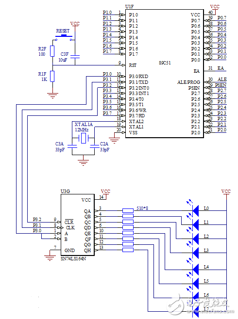
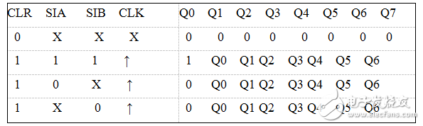
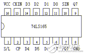
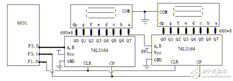
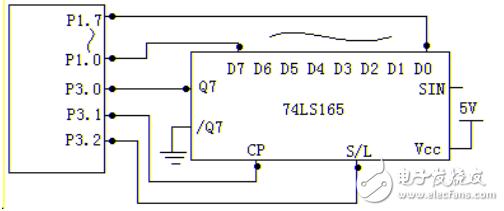
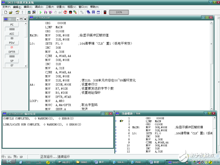
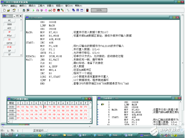
This experiment uses 74LS164 to convert the input serial number into parallel number output. 74LS164 is the serial input parallel output shift register. Its pin diagram and function are as follows: A, B: serial input; QA ~ QH: parallel output; CLR: Clear end, active low; CLK: clock pulse input, rising edge is valid. The experiment adopts serial operating mode 0 and P1 port to output data serially. When the serial port operation mode is 0, the data is 8 bits, which is output from the RXD terminal. The TXD terminal outputs a shift signal, and its baud rate is fixed at Fosc/12. The transmission starts immediately after the CPU writes data to the SBUF register. After the 8-bit data is input, the hardware sets the TI bit of the status register and TI must be cleared by software. Serial port operation mode 0 data/clock is automatically shifted output. When using P1 port to output data, it is necessary to program the displacement data, each output a data bit, and then output a shift pulse. Content and steps: This experiment needs to use the minimum system (F1 zone), 16-bit logic level display (I4 zone) and 74LS164 (G3 zone). 1. Select the 89C51 microcontroller minimum application system module, connect the 74LS164 parallel output JD5G and the 16-bit logic level display module JD2I with eight data lines, and connect the 74LS164 serial input A/B (1 and 2 pins) On RXD, CLK is connected to TXD and CLR is connected to INT0. 2. Use a serial data communication cable to connect the computer to the emulator. Insert the emulator into the module's locking socket. Note the emulator's orientation: the notch is facing up. 3, open KeiluVision2 simulation software, first create the project file of the experiment, then add the "TH23_74164.ASM" source program, compile until compiled correctly. 4. Run the program at full speed. Observe that the LED is on and off. Move it right twice before moving twice and then twice. 5. The source program can also be compiled into an executable file and burned into the 89S52/89S51 chip with an ISP burner. Experiment content 1. Use the 74LS164 chip to expand the parallel output port. In this experiment, we use the 74LS164 to expand the interface display circuits of two 8-bit output ports. The two digital tubes display the numbers between 00 and 99. 2. Use the 74LS165 chip on the experimental system to program 8-bit data parallel input and serial port serial receive, and store the received data in the CPU internal memory area 50H~59H for a total of 10 data. (parallel input data is sent from port P1) Programming Guide 1, 74LS164 string in and out experiments. (1) In this experiment, when the serial port of MCS-51 microcontroller works in the transmission state of mode 0 (shift register mode, used for parallel I/0 port expansion), the serial data is sent from P3.0 (RXD). The bit clock is sent by P3.1 (TXD). Under the action of the shift clock, the serial port transmit buffer data is shifted into the 74LS164 bit by bit. It should be pointed out that since the 741S164 has no parallel output control terminal, the status of the output terminal will change continuously during the serial input process. Therefore, in some applications, the output terminal of the 74LS164 should be connected to output three-state gate control. In order to ensure the end of the serial input and then output the data. (2) 74LS164 pin function table 2,165 parallel string conversion experiments. (1) 74LS165 chip pinout Pin description: D0throughD7--Parallelinputs SI--Serialinput Q7,/Q7--Dataoutputs CLK--Clock CKIN--Clockinhibit S/L--(high effective) Shift/Parallel-load control (active low) (2) Programming instructions The 74LS165 is an 8-bit parallel placement shift register. When the shift/input (S/L) transitions from high to low, the data at the parallel input is placed in the register; when S/L=1, and the clock disable pin (pin 15) is low, The clock input is allowed. At this moment, under the action of the clock pulse, the data is shifted from D0 to D7. In the following circuit schematic, TXD (P3.1) as a shift pulse output is connected to all 74LS165's shift pulse input CP; RXD (P3.0) as a serial input and the 74LS165's serial output Q7 Connected; P3.2 is used to control the 74LS165's shift and placement while connected to the S/L; the 74LS165's clock inhibit terminal (15 pin) is grounded to allow clock input. When extending multiple 8-bit parallel inputs, the two chips start and end (Q7 and Sin). Experimental wiring diagram 1. 74LS164 string in and out experiment 2,165 parallel and serial conversion experiment Experimental procedure 1. In the 74LS164 serial-in and parallel-out experiment, use the double head wire connection, connect P3.0 to the jack A/B, P3.1 to the jack CP, and P1.0 to the jack/CLR, transfer to the program run, two The digits on the digital tube display the numbers 00~99. The following is the situation of the 74LS164 serial in and out program running simulation: 2. In the 165 parallel-to-serial conversion experiment, P1.0 to P1.7 are connected to D7 to D0, P3 .0 to Q7, P3.1 to CP, and P3.2 to S/L. Load the program 165.ASM, compile, load, and run. Check if the data in CPU internal memory 50H~59H is 01H~0AH (Note that the memory is refreshed). The following is a 165 parallel serial conversion program simulation running: program 1, 74LS164 string in and out experimental program ORG 0000H LJMP MAIN ORG 0100H MAIN: MOV 30H, #00H ; Assign initial value to display buffer MOV 31H, #00H L0: SETB P1.0 ;164 Clear terminal 'CLR' set to 1 (active low) INC 30H MOV A, 30H CJNE A, #0AH, AA MOV 30H, #00H INC 31H MOV A, 31H CJNE A, #0AH, AA MOV 30H, #00H MOV 31H, #00H ; Changes the contents of 31H, 30H cells in 00 to 99 cycles AA: MOV SCON, #00H ; Setting serial port MOV R7, #02H ; Set the number of bytes to send MOV R0, #30H ; Set address pointer MOV DPTR,#TAB LOOP: MOV A, @R0 MOVC A, @A+DPTR ; Remove font code MOV SBUF,A ;Send WAIT: JNB TI, WAIT ; Waiting for the completion of a frame CLR TI INC R0 ;points to the next word code DJNZ R7, LOOP MOV R2, #30H ; Call Delay Subroutine LCALL DELYA CLR P1.0 ;164 Clear 'CLR' Set to 0 (Active Low) SJMP L0 TAB: DB 3FH,06H,5BH,04FH,66H,6DH,7DH,07H,7FH,6FH ;7-segment LED segment code (common cathode) DB 77H, 7CH, 39H, 5EH, 86H, 8EH, 0FFH, 0F1H, 0C6H, 092H, 0BFH DELYA: PUSH 02H ; Delay subroutine DELYB: PUSH 02H DELYC: PUSH 02H DELYD: DJNZ R2,DELYD POP 02H DJNZ R2, DELYC POP 02H DJNZ R2,DELYB POP 02H DJNZ R2, DELYA RET END 2,165 parallel and serial conversion experiment program ORG 0000H LJMP MAIN ORG 0500H MAIN: MOV R7, #10 ; Set the number of parallel read data to 10 MOV R0, #50H ; Set internal RAM data area first address, receive external parallel input data MOV 40H, #00H START: INC 40H MOV P1, 40H ; Use the data output from Port 1 as the parallel input of 74LS165 CLR P3.2; Parallel placement of data, S/L=0 SETB P3.2 ; Allow serial shift, S/L=0 RXDATA: MOV SCON,#10H ; Set the serial port mode 0 to allow receiving and start the receiving process WAIT: JNB RI, WAIT ; A frame was not received and the loop waited CLR RI; Clear RI logo, ready for the next reception MOV A, SBUF ; Read in data MOV @R0,A ; Sent to RAM Buffer INC R0 ; points to the next address DJNZ R7,START ; 10 data have not been read and re-injected in parallel SJMP $; 10 data read, the program in place loop END ; Check CPU internal memory area 50H~59H data is 01~0AH The LTM series is designed to meet the needs of human-computer interaction in the market. Our engineers have developed 8-inch to 65-inch LCD touch monitors and touch all-in-ones to provide longer life, high picture quality, and a wide temperature range. It can be used for uninterrupted operation in rugged equipment in harsh environments (high and low temperature, humidity, salt spray and rain) and harsh conditions (high shock, high vibration, and fall). Support a variety of signal input interfaces, including VGA and Video, special requirements can increase DVI and HMI interfaces; support DC12V or AC220V power input, special requirements support DC 9 ~ 36V wide voltage input can be wall-mounted, folding / rotating bottom seat Embedded installation, open installation and other diversified installation methods to meet the various needs of customers. Specially designed folding base, adjustable for multiple angles; no shaking when touched; TFT digital true color LCD display mode to meet customer visual effects; hidden adjustment panel to make the frame more smooth and flat; touch screen can flexibly choose serial port, The USB port communicates with the host, using resistive screens, sonic screens, and infrared screens to meet customer environmental needs. desktop display,desktop monitors,desktop monitor touch screen,desktop monitoring,best desktop monitors,desktop computer monitor Shenzhen Hengstar Technology Co., Ltd. , https://www.angeltondal.com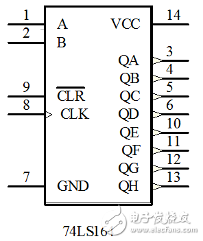
74ls164 and MCU serial and parallel conversion (string and \ string in and out)
74LS164 string and experiment