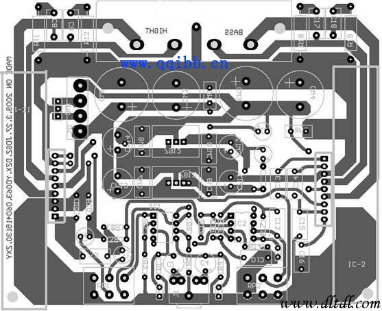
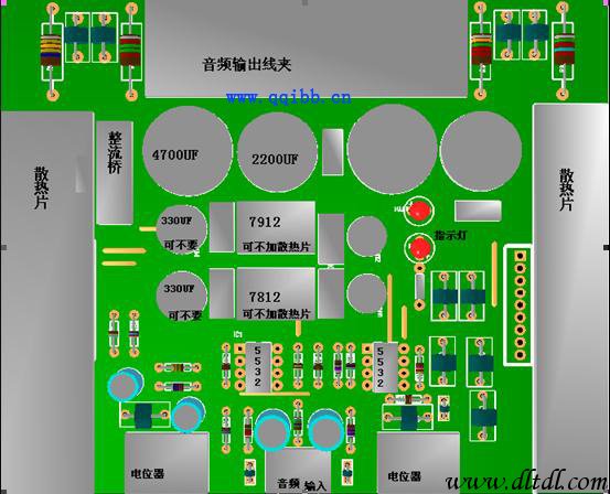
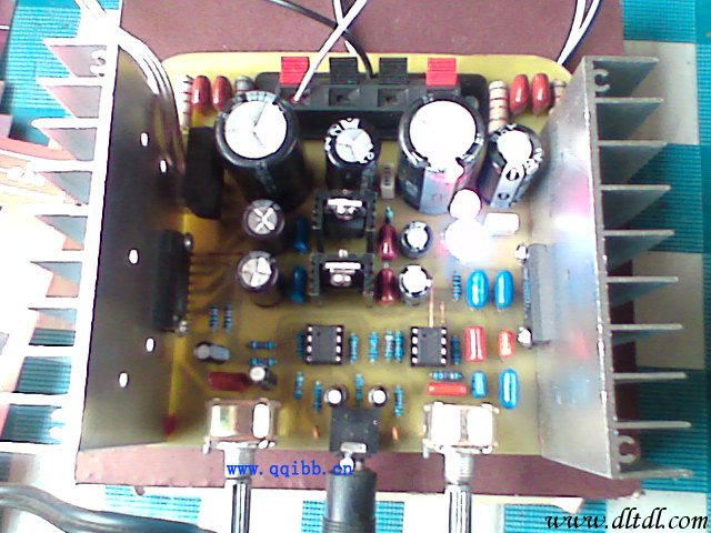
The circuit is a 10 × 12 cm board, and there are several important considerations when working on it: Most of the components used are custom-made. I used a 40-mil line width for the front signal lines. Power lines can be thickened once the initial wiring is complete. The output lines of the power amplifier block should also be widened for better performance. Ground wires should be thickened as well to reduce the impedance of the components to ground. Ordinary resistor-capacitor pads use 80-mil solder holes with a 30-mil diameter. Rectifier bridge pads have a 190-mil solder hole with a 60-mil diameter. Potentiometer pads are 120-mil with a 60-mil solder hole; ensure correct orientation during packaging, with pin 1 grounded and pin 2 as the adjustable end. Audio socket pads are 120-mil with a 50-mil solder hole. TDA1521 is packaged in SIP9 format with pad dimensions X=100mil and Y=80mil. NE5532 uses DIP8 package with pad dimensions 90mil and a 32-mil solder hole. LM7812/LM7912 pads are 85mil with a 40-mil solder hole. Other components should be modified based on their specific requirements. Jumper wiring: Jumpers are often placed under large components for aesthetic reasons when drawing PCB layouts. They must be soldered before mounting the components. A jumper can be a single thick wire or a pin cut from another component. Resistor welding: According to the assembly drawing, all resistors are installed and soldered in their respective positions, and the cut resistor leads are reserved for use as the next jumper. Welding of integrated block bases: The two NE5532 integrated blocks are mounted on the integrated block bases. Do not solder the integrated block directly to the circuit board; the base must be soldered first. Note: Pin 1 should face the upper left corner. Electrolytic capacitors, 7812, 7912, and LEDs: These components are directional, so special attention must be paid during installation. Special handling of integrated blocks: Heat dissipation from 7812 and 7912 is minimal without a heatsink. If a heatsink is added, ensure it is not grounded. For example, the heatsink of the 7912 connects to the input, while the TDA1521 heatsink connects to the negative power supply. Short circuits with the board could have severe consequences. When fixing the heatsink, ensure proper insulation between the copper and the circuit board. Due to high power consumption, the TDA1521 requires a larger heatsink (an 8cm x 5.5cm finned heatsink was chosen). My 3D renderings: Sample: This project has been a rewarding experience, combining technical precision with creative design. Working on the PCB layout taught me the importance of careful planning and attention to detail. The choice of components and their placement were critical, especially considering the power requirements and thermal management of the TDA1521. It’s fascinating how each component contributes to the overall functionality of the circuit, and seeing the final product come together has been incredibly satisfying. I look forward to experimenting with more advanced designs in the future!
Features
â—† Designed For Water and Dust Tight(IP67)
â—† Customized Designs
Micro Lever Switch,Enec Micro Switch,Ip67 Rotary Switch,Snap Action Micro Switch Ningbo Jialin Electronics Co.,Ltd , https://www.donghai-switch.com
â—† UL&ENEC&CQC Safety Approvals
â—† Long life & high reliability
â—† Variety of Levers
â—† Wide Range of wiring Terminals
â—† Wide used in Automotive Electronics,Appliance and Industrial Control etc.