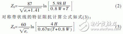
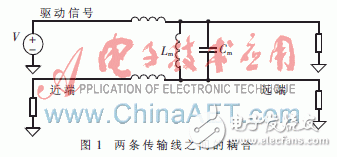
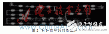
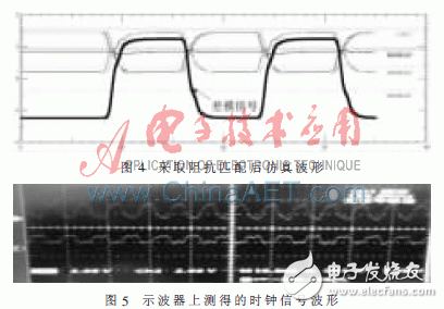
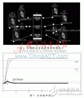
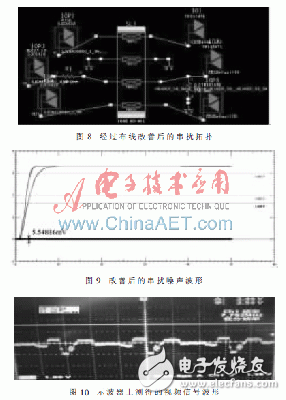
Advances in semiconductor technology have led to an increasing scale of chip integration, and the clock frequency of the chip is getting higher and higher, resulting in shorter signal rise/fall times. When the clock frequency exceeds 50 MHz, the signal trace of the PCB must be considered by the transmission line. 1 Signal Integrity Overview Signal integrity is the ability of a signal to respond in the circuit with the correct timing and voltage. Conversely, if the signal does not respond at the correct timing and voltage level in the circuit, it means that signal integrity issues have arisen. Reflection and crosstalk are the more common factors leading to signal integrity problems [1]. Reflection is the echo on the transmission line. If the impedance on the transmission line is not continuous, it will cause reflection of the signal. The size of the reflected signal component is mainly determined by the reflection coefficient [2]. The reflection coefficient is calculated as equation (1): Among them, Z0 is the characteristic impedance of the transmission line, and Zt is the impedance that causes discontinuity. The characteristic impedance Z0 of the transmission line is defined as the ratio of voltage to current at any point on the transmission line. In PCB design, the transmission line mainly considers both microstrip lines and strip lines. Therefore, when calculating the characteristic impedance, it should be approximated according to the corresponding transmission line type [3]. The characteristic impedance calculation formula of the microstrip line is as shown in equation (2): Where W (mm) is the conductor width, T (mm) is the conductor thickness, H (mm) is the dielectric thickness, and εr is the dielectric constant of the board material. Crosstalk refers to the undesired noise voltage interference signal generated on adjacent signal lines due to the mutual coupling of electromagnetic fields when the signals propagate on the transmission line, that is, the energy coupling between different transmission lines. As shown in Figure 1. Crosstalk is the result of the combined action of mutual capacitance Cm and mutual inductance Lm. It is generally defined that the crosstalk of the interfered transmission line near the end of the driver is near-end crosstalk (also called backward crosstalk), and the crosstalk of the interfered transmission line away from the end of the driver is far-end crosstalk (also called forward crosstalk) [4]. Mutual inductance, that is, inductive coupling, is electromagnetic interference caused by a magnetic field generated by a current change on a driven transmission line causing an induced voltage on a transmission line that is not driven. The magnitude of the mutual inductance Lm can be calculated by equation (4): 2 Signal integrity solutions 2.1 Reflex measures Reflections on the transmission line can have a serious negative impact on the performance of digital systems. Therefore, effective measures must be taken to suppress the reflection. According to the reason of reflection, there are essentially three ways to reduce the influence of reflection: (1) reduce the system frequency; (2) shorten the PCB trace; (3) terminate one end of the transmission line and match the characteristic impedance of the transmission line. Impedance to eliminate reflections. In contrast, only the third method is more reasonable. There are two main strategies for impedance matching: (1) matching at the load end, that is, parallel termination matching; (2) matching at the source end, that is, serial termination matching. From a system design perspective, strategy (1) should be preferred because it eliminates reflections before signal energy returns to the source, eliminating one reflection, reducing noise, electromagnetic interference (EMI), and radio frequency interference (RFI). Strategy (2) is relatively simple to implement and widely used in practice [7]. 2.2 Crosstalk resolution measures Crosstalk is the result of a combination of factors. It is impossible to completely eliminate crosstalk in the PCB design, and only effective measures can be taken to minimize it, as long as the crosstalk is suppressed within the allowable range of noise. By analyzing the causes of crosstalk, the following measures can be taken to suppress crosstalk during PCB design: in the case of sufficient space, the distance between the wires can be increased as much as possible; and the parallel length of the wires between adjacent networks should be minimized; Wiring between the two layers should be done with vertical wiring to reduce crosstalk between adjacent layers; ground lines can be inserted between the two lines, or critical signal lines can be shielded with grounding wires [8, 9]. 3 Signal integrity simulation results analysis 3.1 The Hardware structure of the system This system uses Samsung S3C6410 processor, the main frequency is up to 667 MHz, and the PCB design adopts 8-layer structure. It mainly uses two 32 MHz DDR SDRAMs, one 128 MHz NAND FLASH, one 32 MHz NOR FALSH, NIC interface, CAMERA standard interface and some other peripheral interfaces. The S3C6410 processor and other chips are highly integrated chips with a wiring width of 3 mils to 4 mils. 3.2 Simulation environment and model At present, there are mainly three major companies' EDA tools for signal integrity simulation analysis, namely Cadence's SpecctraQuest, Mentor's Hyperlynx and Ansoft's SIwave [10]. Since the PCB of the entire system is designed using Cadence tools, this paper selects SpecctraQuest as the software for simulation analysis. The device models used for board level simulation are mainly spice and IBIS. As a behavioral model, IBIS has been verified by practice to fully meet the accuracy required for simulation analysis. Therefore, the simulation model of this system uses the IBIS model. 3.3 Analysis of simulation results 3.3.1 Reflection Simulation Analysis In this system, the differential clock signals SCLK and SCLKN from S3C6410 to DDR SDRAM have a frequency of up to 133 MHz, which is a very critical signal. The network topology is shown in Figure 2. Through simulation analysis, the signal quality is poor when impedance matching is not performed. Figure 3 shows the differential signal waveform. It can be seen from Fig. 3 that the differential mode signal waveform of the differential pair receiving end is severely distorted. Therefore, impedance matching is required, and a single-resistance crossover matching method is adopted. By considering the entire differential network topology, using equations (1), (2), and (3), the final matching impedance value is approximately 470 Ω. The differential signal waveform after single-resistance cross-matching is shown in Figure 4. As can be seen from Figure 4, the differential mode signal after impedance matching has good signal integrity. Figure 5 shows the measured clock signal waveform. 3.3.2 Crosstalk simulation analysis The video signal of this system is also a key signal and is more sensitive to noise. Therefore, it is necessary to suppress the crosstalk noise of the adjacent networks (XEINT0_KPROW0_GPN0 and XM0RNB) of the video signal network XDACOUT_0. Figure 6 is a crosstalk topology model without routing improvements. The signal waveform of the XDACOUT_0 network is monitored by sending a high-level pulse to the XEINT0_KPROW0_GPN0 and XM0RNB networks. The crosstalk noise waveform of the XDACOUT_0 network is shown in Figure 7. The crosstalk noise reaches 219.735 mV, which is unacceptable. Therefore, relevant crosstalk suppression measures must be taken to improve the wiring. According to the actual situation of the board wiring space, by increasing the spacing between XDACOUT_0 and the adjacent network, the length of the parallel traces is reduced, and the grounding line is shielded between the networks XDACOUT_0 and XM0RNB. After the above measures are taken to improve the wiring, the extracted topology is as shown in FIG. 8. The improved crosstalk noise waveform is shown in Figure 9. As can be seen from the figure, the crosstalk noise is only 5.5481 mV, which is well suppressed and meets the design requirements. Figure 10 shows the measured video signal waveform. This paper discusses the causes of crosstalk and reflection by introducing signal integrity theory. Using Cadence's software SpecctraQuest, the S3C6410 based on ARM11 architecture is used as the main processor embedded system for signal integrity simulation analysis. The reflection problem of the differential clock signal of the DDR SDRAM and the crosstalk problem of the video signal are solved. The clock signal and video signal of the embedded system after actual debugging meet the design requirements, and the system can work stably. Therefore, in high-speed circuit design, the use of signal integrity theory for simulation analysis is of great significance for guiding engineering practice. Power Source,arcade power supply switch,power supply for game,vending power supply Guangzhou Ruihong Electronic Technology CO.,Ltd , https://www.callegame.com![]()