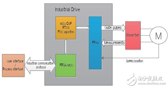
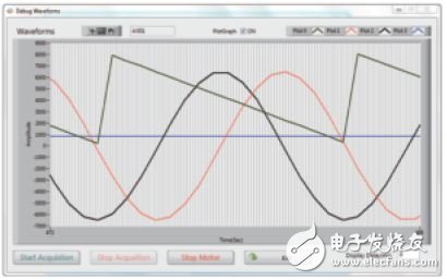
Recent developments in the industrial market have driven the need for highly integrated, high performance, low power FPGA devices. Designers prefer network communications rather than peer-to-peer communications, which means additional controllers may be required for communication, which indirectly increases BOM cost, board size, and associated NRE (one-time engineering cost) costs. Total cost of ownership is used to analyze and estimate the life cycle cost of the acquisition. It is an extended set of all design-related direct and indirect costs, including engineering cost, installation and maintenance costs, bill of materials (BOM) costs, and NRE (R&D) Cost, etc. By considering system-level factors, it is possible to minimize total cost of ownership, resulting in sustainable long-term profitability. Microsemi offers SmartFusion2 SoC FPGA devices with hard-core ARM Cortex-M3 microcontrollers and IP integration in a cost-optimized package with features that reduce BOM and board size. With low power consumption and a wide temperature range, these devices operate reliably in extreme conditions without a cooling fan. The SmartFusion2 SoC FPGA architecture integrates a hard-core ARM Cortex-M3 IP with the FPGA fabric for greater design flexibility and faster time-to-market. Microsemi offers an ecosystem of multiple multi-axis motor control reference designs and IP for motor control algorithm development, making it easier to move from multi-processor solutions to single-device solutions (ie SoC FPGAs). Factors affecting TCO The following are some of the factors that affect the system TCO. (1) Long life cycle. FPGAs can be reprogrammed after deployment in the field, which extends the life cycle of the product, allowing designers to focus on new product development and achieve faster time to market. (2) BOM. Microsemi's flash-based FPGAs do not require a startup PROM or flash MCU to load the FPGA at power-up. They are zero-level nonvolatile/instant-on devices. Unlike SRAM-based FPGA devices, Microsemi's flash-based FPGAs do not require an additional power-up monitor because flash switches do not change with voltage. (3) Time to market. Intense competition among OEMs urgently requires more product differentiation and faster time to market. Proven IP modules dramatically reduce design time. It is now possible to provide multiple IP modules for building industrial solutions, while more modules are under development. Another unique advantage that SoC demonstrates is that it can be used to debug FPGA designs. To debug the FPGA design, the microcontroller subsystem can be used to extract information from the FPGA through a high-speed interface for debugging. (4) Engineering tool costs. Contrary to the expensive concept of FPGA development tools, Microsemi offers a free Libero SoC IDE for FPGA development that only pays when developing high-end devices. Industrial drive system The industrial drive system consists of a motor control device that contains the logic and protection logic that drives the inverter, and a communication device that enables the supervisory control to initialize and modify the runtime parameters. Figure 1: Typical industrial drive system. In a typical drive system (Figure 1), multiple controller devices may be used to implement the drive logic. One device may perform calculations related to motor control algorithms, the second device may run communication-related tasks, and the third device may perform safety-related tasks. Multi-axis motor control Traditionally, industrial motor control applications use microcontrollers or DSPs to run the complex algorithms required for motor control. In most traditional industrial drives, FPGAs are used with microcontrollers or DSPs for data acquisition and fast-action protection. . In addition to data acquisition, PWM generation, and protection logic, FPGAs have traditionally not played a major role in implementing motor control algorithms. The method of implementing a motor control algorithm using a microcontroller or DSP is not easily extended to multiple motors operating at independent speeds (multi-axis motor control). The Microsemitech SmartFusion2 SoC FPGA can be integrated and complete with multiple devices using a single device. Motor drive control (Figure 2). Figure 2: The Microsemitech SmartFusion2 SoC FPGA uses a single device for complete multi-axis motor drive control. Control can be divided into two parts. One part is used to run field oriented control (FOC) algorithms, speed control, current control, speed estimation, position estimation, and PWM generation; the other part includes speed profiles, load characteristics, process control, and protection (faults and alarms). The implementation of the FOC algorithm is time critical and needs to be performed at very high sampling rates (in the microsecond range), especially for high speed motors with low stator inductance. This makes it more advantageous to implement FOC algorithms in FPGAs. Process control, speed profiles, and other protections do not require fast updates, so they can be executed at lower sample rates (in the millisecond range) and can be programmed in the built-in Cortex-M3 subsystem. The transistor switching period plays an important role in the drive. If the FOC loop execution time is much shorter than the switching period, the hardware module can be reused to calculate the voltage of the second motor. This means that the device can deliver higher performance at the same cost. Figure 3: Field Oriented Control (FOC) block diagram of a permanent magnet synchronous motor. (1) Motor control IP module. Figure 3 shows the sensorless field oriented control algorithm, which is discussed in this section and is provided as an IP core. ◠PI controller. The proportional integral (PI) controller is a feedback mechanism for controlling system parameters. It has two adjustable gain parameters - proportional and integral gain constants for controlling the dynamic response of the controller. The proportional component of the PI controller is the product of the proportional gain constant and the error input, and the integral component is the product of the cumulative error and the integral gain constant. These two components are added together. The integration phase of the PI controller may cause instability in the system because the data values ​​increase uncontrollably. This uncontrolled rise in data is called integral saturation, and all PI controller implementations include an anti-frozen mechanism to ensure that the controller output is limited. Microsemi's PI controller IP module uses the hold-on-saturaTIon algorithm for anti-shaking. This module also provides additional features to set the initial output value. ◠Field Oriented Control (FOC). The FOC is an algorithm that provides optimal current to the motor by independently determining and controlling the torque and magnetization current components. In a permanent magnet synchronous motor (PMSM), the rotor has been magnetized. Therefore, the current supplied to the motor is only used for torque. FOC is a computationally intensive algorithm, but the Microsemi's motor control reference design has been built for optimal use of device resources. The FOC algorithm includes Clarke, Park, inverse Clarke, and inverse Park transform. ◠Angle estimation. One input to the FOC is the rotor angle. Accurate determination of the rotor angle is essential to ensure low power consumption. Adding physical sensors that determine position and speed increases system cost and reliability. Sensorless algorithms help eliminate sensors but increase computational complexity. Microsemi offers two angle calculation algorithm IP modules for sensorless control - one based on the Luenberger observer and the other based on direct back EMF calculations. The company also offers a separate reference design based on Hall sensors and encoders. ◠PLL.PLL is used to synchronize signals and is useful in many applications, such as angle estimation of the inverter and grid synchronization. ◠Rate limiter. The rate limiter module can implement smooth changes to system variables or inputs. For example, in a motor control system, if the speed required by the motor suddenly changes, the system may become unstable. To avoid such situations, the rate limiter module is used to transition from the initial speed to the desired speed. The rate limiter module can be configured to control the rate of change. ◠Space vector modulation. The space vector modulation module improves DC bus utilization and eliminates short pulses from transistor switches. Because the transistor turn-on/turn-off time is longer than the pulse duration, short pulses can cause incorrect switching behavior. ◠Three-phase PWM generation. At the end of all calculations, a three-phase motor voltage is available. These voltages are used to generate the switching signals of the transistors in the inverter. The PWM module generates switching signals for six (three high-side and three low-side) transistors with advanced features such as dead time and delay time insertion. The programmable dead time insertion feature helps to avoid catastrophic short circuits on the inverter pins. The programmable delay time insertion feature allows ADC measurements to be synchronized with PWM signal generation. The module can be configured to operate with an inverter consisting only of N-MOSFETs or an inverter comprising both N-MOSFETs and P-MOSFETs. (2) Debug the FPGA design in the SoC. In general, debugging a design on a microcontroller is relatively simpler than debugging on an FPGA. In SoCs, you can take advantage of the high performance of FPGAs while maintaining the advantages of faster debugging in microcontrollers. The microcontroller subsystem and FPGA architecture in the Microsemitech SmartFusion2 SoC FPGA can communicate with each other via the AMBA APB or AXI bus. This allows test data to be injected into the FPGA fabric or debug data from the FPGA fabric to help visualize internal data for runtime and for real-time debugging. The firmware code can be run in a single step, and breakpoints can be set in the code to analyze the FPGA register data. The multi-axis motor control solution based on SmartFusion2 SoC FPGA is connected to the host PC via USB and communicates with the graphical user interface (GUI) to start/stop the motor, set motor speed values ​​and other system parameters, and draw up to four system variables Such as motor speed, motor current and rotor angle (Figure 4). Figure 4: Screenshot of the GUI - plot internal parameters: rotor angle (green), Valpha (red), Vbeta (black), motor speed (blue). (3) Ecosystem. Microsemi offers a rich set of IP libraries, including several motor control functions discussed earlier. These modules can be easily customized and can be ported in Microsemi devices. Using the Smart Design tools of the Libero SoC software, these modules can be graphically configured and connected together. With these IP blocks, designers can significantly reduce the time required to implement motor control algorithms in an FPGA. These IP modules have been tested on motors running at up to 30,000 r/min and 200 kHz switching frequency. Industrial communication protocol The trend in industrial networks is to replace point-to-point communications by using faster network communications. Achieving such high-speed communications requires support for higher bandwidth, which is not easy for microcontrollers or DSPs that simultaneously process motor control algorithms. In most cases, an additional microcontroller or FPGA is used to handle communication with each motor controller. Commonly used Ethernet-based protocols are the PROFINET, EtherNet/IP and EtherCAT standards, which are still evolving. Other protocols include CAN and Modbus. The advantage of using SoCs in this case is to support multiple Industrial Ethernet protocol standards on a single FPGA platform. Depending on the end system goals, the cost of the system can be optimized by reusing IP and protocol stacks (for communication), or by carefully demarcating functionality in hardware (FPGA) and software (ARMCortex-M3 subsystem). Microsemi's SmartFusion2 FPGAs have built-in CAN, Hi-Speed ​​USB and Gigabit Ethernet modules as part of the microcontroller subsystem. The high speed SERDES module is used to implement protocols involving serial data transfer. safety SmartFusion2 SoC FPGA devices feature several design and data security features. Design security features such as DPA certification anti-tamper protection and encryption features can help protect customers' intellectual property. SoC FPGA devices also include data security features such as ECC hardware accelerators, AES-128/256 and SHA-256 services. For data security, EnforcIT IP Suite and CodeSEAL software security components can be used. EnforcIT IP includes a customizable kernel (as a netlist) that effectively moves the security layer into the hardware. CodeSEAL injects countermeasures into the firmware, can be used independently, or used as an enhancement to EnforcIT. The flexibility of implementing protocols allows designers to use multiple layers of security to authenticate information entering from a central monitoring controller. reliability The growth of security standards across multiple markets drives the need for high reliability. SmartFusion2 is designed to meet the needs of high availability, security critical and mission critical systems. The following are some of the reliability features offered by SmartFusion2 SoC FPGAs. (1) Single-event upset (SEU) immune zero FIT rate configuration. High reliability operation requires SEU immune zero FIT rate FPGA configuration, SmartFusion2 architecture has immunity from alpha or neutron radiation because it uses flash memory to configure the transistors used in routing matrices and logic blocks. SRAM-based FPGAs may have a FIT (time-failure) rate at sea level of 1k to 4k, which is much higher at 5,000 feet above sea level. High reliability applications can accept FIT rates below 20, making SmartFusion 2 best suited for these applications. (2) EDAC protection. SmartFusion2 devices feature an Error Detection and Correction (EDAC) controller that prevents single-event rollover errors in the microcontroller subsystem (MSS) memory. (3) No external configuration device. In complex systems with a large number of FPGAs, using externally configured devices reduces reliability. At power-up, FPGAs take time to configure, which introduces design complexity in applications that use multiple FPGA devices. The SmartFusion2 SoC FPGA includes configuration memory inside the device, which provides the added benefit of turning it on when the device is powered up. (4) Military temperature class devices. The SmartFusion2 SoC FPGA device is fully tested for military temperature conditions. Military-grade devices have 10k and 150k logic units with security features and data security features that allow access to cryptographic accelerators. to sum up The Microsemitech SmartFusion2 SoC FPGAs offer several features that reduce the TCO of industrial designs using highly optimized motor control IP blocks and proven reference designs. Customers migrating from microcontrollers will be able to reuse some of the old code, and FPGA designers will be able to leverage the FPGA fabric and the ARM Cortex-M3 subsystem to create an efficient architecture that allows the motor control and communication modules to reside simultaneously in a single In the device. The presence of the ARM Cortex-M3 microcontroller subsystem enables flexible design and intelligent partitioning while optimizing for performance and cost. The microcontroller subsystem also injects and records data at runtime to speed debug FPGA design. The SmartFusion2 platform also offers a wide range of options for implementing industrial communication protocols. It also provides multiple security features for design and data security, as well as features that meet high reliability requirements. The SmartFusion2 family of devices is backed by powerful ecosystem support to help customers develop industrial solutions with minimal TCO. 2G7 base type LED Tube Light contain 6W and 8W. LED tube light, fits to universal socket base and can replace 24W CFLs downlight without changing ballast. Using polycarbonate to the thermostable cover with chemical synthesis technology, transmittance can be possiblely reach up to 95%. Special anodized surface accelerates cooling rate and has metal texture. High thermal aluminium base board including 3-5% magnesium can accelerate heat dissipation. LED tube series more superior to the traditional lights many times, long life span.Such as energy saving light,commercial lighting. 2G7 Tubes,White 2G7 Tubes,Tube 9W 2G7,17W 2G7 Tubes SHENZHEN KEHEI LIGHTING TECHNOLOGY CO.LTD , https://www.keheiled.com