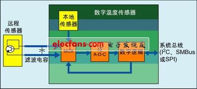
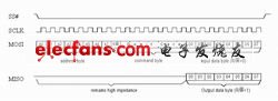
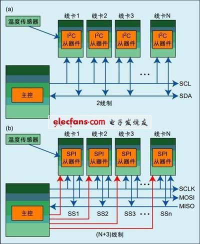
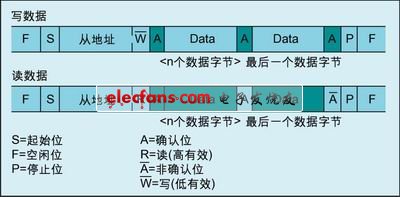
Thermistors, thermocouples, analog silicon temperature sensors, and nickel/platinum resistive temperature detectors (RTDs) require calibration to achieve the desired temperature accuracy. Digital temperature sensors as mixed-signal devices do not require calibration. They have integrated digital logic and operate over a temperature range of -55°C to 50°C. The absolute temperature ratio (PTAT) circuit is used to sense the base-emitter voltage of the diode. (VBE) changes to measure local/remote temperature. It has simple integrated hardware to hold temperature values ​​and program temperature setpoints, device operating modes, sleep modes, and fast/slow slew rates. Data is communicated via an inter-IC bus (I2C bus), a system management bus (SMBus), or a serial peripheral interface (SPI). Specifically, the main components of a digital temperature sensor include a dual current source, a delta-sigma A/D converter, digital logic, and a serial interface to a digital device (such as a microprocessor or microcontroller). (such as I2C bus, SMBus or SPI). There are two types of digital temperature sensors: local or remote temperature sensors, which use a method to force two proportional currents through a diode-connected NPN or PNP transistor, both for measuring the resulting VBE change, using Δ - The A/D converter samples the voltage and converts the value to a digital format. The forced current is generally in a ratio of about 10:1. By forcing the application of the proportional current and measuring the difference between the two VBEs, the first-order effect of the IS-related process-related parameters on the diode can be eliminated. Each temperature sensor is adjusted during production to match the ideal parameters of the diode to be used. The characteristics of the remote diode are taken from the 2N3904/6. Since the local temperature sensor is a simple NPN or PNP structure on a silicon substrate, the remote temperature sensor almost always integrates a local temperature sensor. Therefore, the role of the remote sensor is almost always the same as the two sensors. The local temperature sensor integrates a thermal diode in the same package. For local sensors, the thermal time constant (ie, the time required to reach 63.2% of the final temperature) is a few minutes, depending on the package and the local diode on the IC substrate. Excessive bus loading or too fast conversion can cause the device to self-heat and affect temperature accuracy. The time required for the temperature data to become available is called the slew rate. This rate is determined by the device's internal oscillator and A/D resolution, typically less than 100 Hz or longer than 10 ms. The faster the conversion rate, the faster the temperature data can be retrieved and the more power the temperature sensor consumes. The slew rate is usually low due to the self-heating effect. Figure 1 shows a simplified block diagram of a remote temperature sensor and/or local temperature sensor. Figure 1: Simplified block diagram of a digital temperature sensor. Advantages of the I2C bus or SMBus temperature sensor The most popular digital temperature sensors are those with a serial bus interface. The choice of temperature sensor bus is highly dependent on which interfaces are available on the selected microprocessor or controller. The choice of controller depends on how much experience the engineer has. For system data that requires frequent data streaming, SPI is preferred because it has a faster clock rate, which can range from a few megahertz to tens of megahertz. However, for system management activities, such as reading temperature sensor readings and querying the status of multiple slaves, or requiring multiple masters to coexist on the same system bus (which is often required for system redundancy), or for low power consumption Application, then I2C or SMBus will be the preferred interface. The following sections describe each of the serial buses and their advantages and disadvantages. 1. SPI SPI is a four-wire serial bus interface, master/slave structure. The four wires are serial clock (SCLK), master-slave-in (MOSI), master-in-out (MISO) and slave (SS). signal. The master device is the clock provider and can initiate a read slave or write slave operation. The master will then talk to a slave. When there are multiple slaves on the bus, a transfer is initiated and the master will pull the slave select line low and then initiate data transmission or reception via the MOSI and MISO lines, respectively. The SPI clock is fast, ranging from a few megahertz to tens of megahertz, with no overhead. The shortcoming of SPI in system management is the lack of flow control mechanism. No matter whether the master device or the slave device confirms the message, the master device cannot know whether the slave device is busy or not. Therefore, intelligent software mechanisms must be designed to handle validation issues. At the same time, SPI does not have a multi-master protocol, and complex hardware and external logic must be used to implement a multi-master architecture. Each slave requires a separate slave select signal. The total number of signals is eventually n+3, where n is the number of slaves on the bus. Therefore, the number of wires will increase proportionally with the number of added slave devices. Also, adding a new slave to the SPI bus is not convenient. For each additional slave device added, a new slave select line or decode logic is required. Figure 2 shows a typical SPI read/write cycle. A read/write bit is followed by an address or command byte. Data is written to the slave device via the MOSI signal and read from the device through the MISO signal. Figure 3 shows the system block diagram of the I2C bus/SMBus and SPI. Figure 2: SPI typical read/write cycle. Figure 3: (a) I2C bus/SMBus system interface; (b) SPI system interface. 2. I2C bus I2C is a two-wire serial bus interface that operates in master/slave mode. The two-wire communication signals are open-drain SCL and SDA serial clock and serial data, respectively. The master device is the clock source. Data transfer is bidirectional, the direction of which depends on the state of the read/write bit. Each slave has a unique 7 or 10 bit address. The master initiates a transfer with a start bit and terminates a transfer with a stop bit. The start bit is followed by a unique slave address followed by a read/write bit. The I2C bus speed is from 0 Hz to 3.4 MHz. It is not as fast as SPI, but it is ideal for system management devices such as temperature sensors. I2C has system overhead, which includes start/stop bits, acknowledgment bits, and slave address bits, but it therefore has a flow control mechanism. The master always sends an acknowledgment bit when it is finished receiving data from the slave unless it is ready to terminate the transfer. The slave always sends an acknowledgment bit when it receives a command or data from the autonomous device. When the slave is not ready, it can hold or stretch the clock until it is ready to respond again. I2C allows multiple masters to operate on the same bus. Multiple masters can easily synchronize their clocks, so all masters use the same clock for transmission. Multiple masters can detect which master is using the bus through data arbitration to avoid data corruption. Since the I2C bus has only two wires, the new slave device only needs to be connected to the bus without additional logic. Figure 4 shows a typical I2C bus read/write operation. Figure 4: Typical read/write operation of the I2C bus/SMBus. 3. SMBus SMBus is a two-wire serial bus that was first commercialized in 1996. It is mostly based on the I2C bus specification. Like I2C, SMBus does not require additional pins. The bus was created primarily to add new features, but only works at 100kHz and is designed for smart battery management applications. It operates in master/slave mode: the master provides the clock, provides a start bit when it initiates a transfer, and provides a stop bit when it terminates a transfer; the slave has a unique 7 or 10 bit slave address. There are some differences in timing characteristics between the SMBus and the I2C bus. First, SMBus requires a certain amount of data retention time, while the I2C bus extends the data retention time internally. SMBus has a timeout function, so when SCL is too low for more than 35 ms, the slave will reset the ongoing communication. Instead, I2C uses a hardware reset. The SMBus has an Alarm Response Address (ARA), so when an interrupt is generated by the slave, it does not immediately clear the interrupt, but remains until it receives an ARA with its address sent by the master. SMBus only works from 10kHz up to 100kHz. The minimum operating frequency of 10 kHz is determined by the SMBus timeout function. USB 3.0 Cable,USB Cable 3.0,USB 3 Type C,USB 3.0 Harness Dong guan Sum Wai Electronic Co,. Ltd. , https://www.sw-cables.com