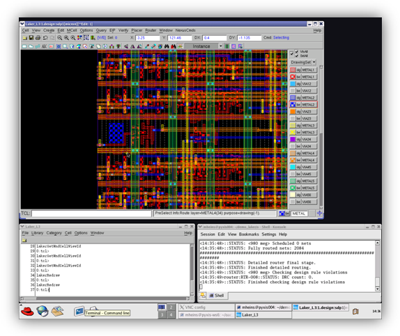
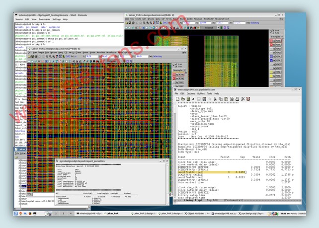
This article details how a digital IC design team at a large fabless semiconductor company in a consumer market can leverage the interoperability of standardized tools to maintain the manual layout benefits of large, performance-oriented 40nm designs. The team has been effectively integrated with Silicon Integration Initiative (Si2)'s OpenAccess (OA) interoperability standardization efforts with the help of multiple vendor tools to form a more productive custom IC layout process. This article refers to the address: http:// Layouts of large digital integrated circuit (IC) designs are typically built using highly automated layout and routing (APR) tools. Although there are many controversies about using APR to replace custom layouts, for most designs, the speed and mastery of APR still outweighs the sacrifice of area or performance; however, designs that require the highest performance or minimum area still rely on " Manually using the custom IC layout method to complete. In a new generation of custom chips, complex rules, tight time-to-market, and slim size and design complexity make the design of the entire custom digital block increasingly difficult to achieve. The fully automated APR process does not provide the necessary control of the layout and routing. Designers need a highly automated and controllable, fully custom digital IC design flow for optimal performance, speed and area. Benefits of Controllable Automation in Custom Design When designing a large number of storage solutions, the design team has been deploying custom IC layout automation for their own simulation and custom digital designs for many years. While analog designers have always used custom design methods, digital design teams typically switch to custom design tools and processes when performance, power, speed, or area requirements exceed the capabilities of APR tools. For optimal performance and turnaround time, engineers use tools with advanced, controllable automation technology to build custom digital designs faster and with less effort. Includes an advanced schematic-oriented layout (SDL) process that uses highly modular, non-dependent process-based parametric cell technology and device-level floorplan tools to provide the speed and control needed to achieve optimal performance and density. There is no need to change the design style or sacrifice the quality of the results. Engineers use the inheritance of the circuit diagram to automatically generate flight lines, and then use built-in rules-oriented interactive winders to manually configure critical network lines to meet the stringent frequency speed requirements of more than 2 GHz. At this level of performance, individual network windings are sensitive to the environment and interactions with other windings, networks, and even layers. To balance these elements, the design team must interact with all the elements of the design environment. When manually winding, the design team can route, extract, and evaluate critical networks for optimal timing and then modify them until the desired value is achieved. Figure 1. Flight line display links and guide rule-oriented manual winding Meeting the challenges of a new generation of custom digital designs Although custom layouts and manual winding methods can meet performance requirements, it is increasingly difficult to complete a new generation of custom digital blocks within a reasonable period of time. As designs become more complex and complex, layout designers encounter serious winding problems and find themselves designing winding paths in an unknown area, and must abandon the density to make manual and point-to-point in increasingly larger blocks. Automated winding operations are properly managed. Although the design team is still able to achieve energy efficiency goals, it often costs to increase the area, which is not satisfactory in a cost-conscious market. In addition, the time required to complete the design far exceeds the time required for a single layout. Figure 2. Interoperability in OpenAccess As the design team moved to the 40nm process to meet increasing performance demands, the challenge also rose. For manual winding and existing automated custom winding solutions, the module becomes too large (too many interconnects) and the design rules are too advanced. There are no mass-customized winders that provide the deep sub-micron DRC-clean and DFM-aware winding technology required for advanced processes. In the beginning, the design team tried to use a hybrid process, using the layout editor to manually wind the critical network as before, and then use APR to support advanced DRC rules for digital winders to complete non-critical networks. Unfortunately, the constant use of multiple tools reduces productivity. Regardless of the efficiency of individual steps, the field of customization and digital design still does not work closely together. In addition, this method is not interactive and can lead to team loss levels and connection data. Most of the automated winders will repeatedly perform the winding of some carefully drawn key networks, requiring extensive manual proofreading and even repeating the winder. Therefore, it takes the design team to work over six weeks to get acceptable, but not the best results. Figure 3. The winder identifies the obstacle and then winds Even in non-critical networks, automated winding can increase the productivity of the design team as long as it does not interfere with the ability to repeat operations. Moreover, it is currently not possible to present the precise spacing limitations required for partial pre-winding and guiding APR tools. Therefore, instead of causing undesirable parasitic effects in the custom module, manual manual rewinding and multiple lengthy re-executions are required. While automation can often increase productivity, it now makes difficult processes more tedious because designers have no control over the results. In fact, manual proofreading of critical networks in a layout that has all been completed is usually more time-consuming than manually winding from scratch. The design team came to the conclusion that in order to achieve optimal results in less time, a heterogeneous environment that maintains hierarchy, connectivity and design integrity through controlled automation is required. Interoperability saves time The standards organization Silicon Integration Initiative (Si2) provides an interoperable database of electronic design automation (EDA) tools, called OpenAccess (OA), which has become the standard for custom design in recent years. OA has a little-known function, the OA Run Time Model (OA-RTM), which can be used as an in-memory model for EDA tools. This means that completely different tools can operate on the same memory agent that designs data at the same time. The tools of many suppliers using OA-RTM can work smoothly as tools provided by a single supplier. With OA-RTM, Pyxis Technology's new high-performance custom winders work in the Laker custom layout environment. This extremely large capacity custom digital winder has been verified by the customer to be able to establish DRC-correct, DFM-aware windings at 45nm and below; it is capable of performing all levels of winding and is progressive, meaning that there is no need to change Manually established both critical networks. When executing a custom IC layout system, the designer can select the chip area and let the integrated winder perform routing of all networks under this constraint. Ports that force a particular winding path, as well as blocks, changes and fixed, and existing windings are all identified by the winder, without the need for data conversion or data storage to disk. Figure 4. Hypothetical analysis of the interactive environment Using this interoperable solution, the design team was able to use automated custom IC layout systems and SDL methods to build layouts as before. The winding of the transistor layer is performed by the layout tool, just like a critical network. Alternatively, pre-wires defining critical network windings can be defined by a layout editor. Winding in stages, starting with a critical network, and then sorting groups (hierarchy), or entire blocks, in just a few minutes can be done in one go. The design team is also able to leverage the built-in extraction and timing engine of the custom winder to quickly feed back parasitic parameters and sample timing. In this way, engineers can determine when the winding topology is "good enough" to avoid over-wiring. Moreover, the speed and controllability of this custom process is very practical, enabling rapid evaluation of the placement of layout elements for optimal results. Winders can also add “dummy fills†(redundant metals, usually inserted into the layout to increase data density for uniformity and flattening), helping to identify possible destructive parasitics to ensure Virtual fillings set by the fab do not cause unexpected problems. Combining these capabilities with a highly automated custom layout system, the design team worked with EDA vendors to create a solution that performs fast, iterative “hypothetical†analysis while optimizing layout and routing. With the ability to repeatedly wind, extract, analyze timing, modify and validate, the design team can reduce the design cost of achieving higher performance goals while reducing power consumption and area – and much longer than previously required for a single layout The time is shorter. Test Results Specific tests involving critical, high-performance blocks previously took six weeks to get an acceptable solution. The performance requirements of such blocks conflict with area and power requirements, making it very difficult to achieve success. In order to confirm the performance of the winder, the existing windings will be removed. Flatten the design in the layout editor and the entire block will be automatically wound in minutes. By mimicking the standard process, an extra version is quickly created, in which the layout of the critical network is manually applied by the layout editor, and then the automated network winder is used to implement the remaining network. In the automated winding program, there is no change to any critical network and no DRC violations. After the initial proof of concept, the design team proved consistent results, and large, high-performance custom digital blocks, which usually take three to six weeks to complete, can now be built in just one week. This means that the design team can free up more time to optimize the performance, area and power of the custom block, ultimately enabling the product to achieve higher value. Carbon fiber heating element Carbon Infrared Heater,Electric Carbon Infrared Heater,APG Carbon Infrared Heater,220V Electric Carbon Infrared Heater Ningbo APG Machine(appliance)Co.,Ltd , http://www.apgelectrical.com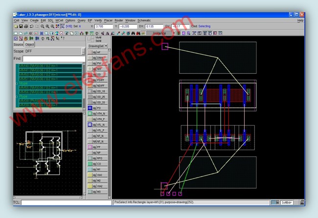

Such products are made of carbon fiber for the heating of the basic material made of tubular heating element, the use of reflective surface heat. The overall type of straight barrel and rectangular floor type: straight through the general use of single tube fever, the body can automatically rotate for the entire room heating. Turn on the power after the heating rate is surprisingly fast, in 1 to 2 seconds when the body has been hot, 5 seconds surface temperature up to 300-700 degrees, power in the 600 ~ 1200W adjustable. Rectangular floor type with double tube heat, you can floor or wall use, power is relatively large, in the 1800 ~ 2000W or so. In addition to heating function, these products can also play the effect of health care therapy. When the heating body heating can produce 765.9W / M of infrared radiation, the equivalent of a spectrum physiotherapy instrument.